
 German
 Japanese
 Portuguese
 Korea
Korea
 Mexico
 Dutch
Dutch


Texas Instruments
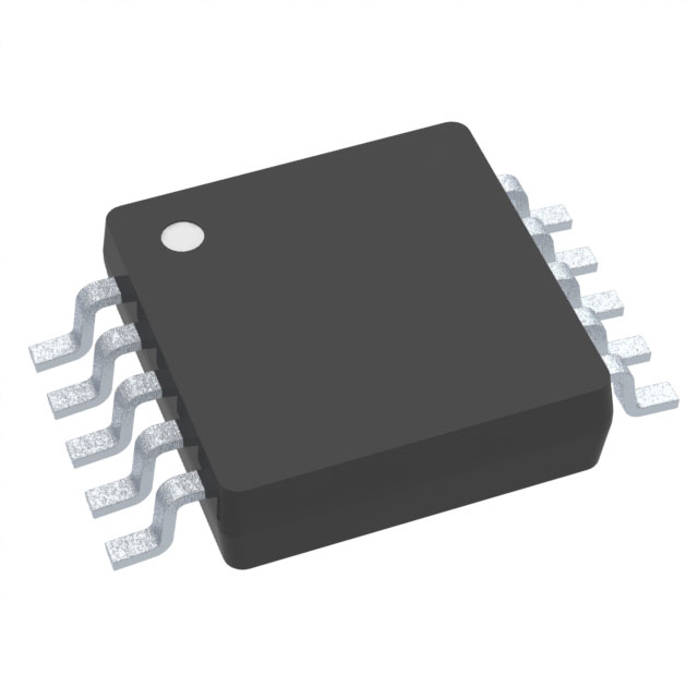
TLV2463IDGS

Why Choose Us?
Professional Platform
B2B & B2C purchasingDelivery at full speed
1-2 days deliveryWide variety
Original manufacturers365 days guarantee
Responsible quality
.png)


Tech Specifications
TLV2463IDGS Description
TLV2463IDGS Description
The TLV2463IDGS is a high-performance, general-purpose operational amplifier designed by Texas Instruments. This dual-channel op-amp is housed in a 10-lead small outline package (VSSOP) and is optimized for surface-mount applications. It features a wide supply voltage range, from 2.7 V to 6 V, making it suitable for a variety of low-power and low-voltage systems. The TLV2463IDGS is known for its excellent performance characteristics, including a gain bandwidth product of 6.4 MHz, a slew rate of 1.6 V/µs, and a low input bias current of 1.3 nA. These attributes make it ideal for applications requiring high precision and low noise.
TLV2463IDGS Features
- Wide Supply Voltage Range: The TLV2463IDGS operates effectively within a supply voltage range of 2.7 V to 6 V, providing flexibility for various low-power applications.
- High Gain Bandwidth Product: With a gain bandwidth product of 6.4 MHz, this op-amp ensures high-frequency performance and stability, making it suitable for signal processing and filtering applications.
- Low Input Bias Current: The low input bias current of 1.3 nA minimizes the impact on sensitive input signals, enhancing the accuracy and reliability of the amplifier.
- High Slew Rate: The 1.6 V/µs slew rate allows for fast response times, making the TLV2463IDGS ideal for applications requiring rapid signal transitions.
- Low Supply Current: Each channel consumes only 550 µA, ensuring efficient power usage and minimal heat generation, which is crucial for compact and power-sensitive designs.
- Low Input Offset Voltage: The input offset voltage of 500 µV ensures high precision and accuracy in signal amplification.
- High Output Current: Each channel can deliver up to 80 mA, providing robust performance and the ability to drive various loads effectively.
- Compliance and Reliability: The TLV2463IDGS is REACH unaffected and RoHS3 compliant, ensuring environmental and regulatory compliance. It also has a moisture sensitivity level (MSL) of 1, making it suitable for unlimited storage and handling.
TLV2463IDGS Applications
The TLV2463IDGS is versatile and finds applications in a wide range of industries and systems:
- Consumer Electronics: Ideal for portable devices, audio equipment, and other consumer electronics where low power consumption and high performance are critical.
- Industrial Control: Suitable for precision control systems, sensors, and instrumentation where accuracy and reliability are paramount.
- Medical Devices: Applicable in medical equipment that requires high precision and low noise, such as diagnostic tools and monitoring devices.
- Automotive Electronics: Can be used in automotive systems for signal processing and control applications, benefiting from its low power and high performance.
- Telecommunications: Effective in communication systems for signal amplification and processing, ensuring high-quality signal transmission.
Conclusion of TLV2463IDGS
The TLV2463IDGS from Texas Instruments stands out as a robust and versatile general-purpose operational amplifier. Its wide supply voltage range, high gain bandwidth product, low input bias current, and high slew rate make it an excellent choice for a variety of applications. The low supply current and high output current further enhance its efficiency and performance. With its compliance to environmental and regulatory standards, the TLV2463IDGS ensures reliability and sustainability. Whether used in consumer electronics, industrial control, medical devices, automotive electronics, or telecommunications, the TLV2463IDGS delivers high precision and performance, making it a reliable choice for engineers and designers.
FAQ
Not available to buy online? Want the lower wholesale price? Please Send RFQ to get best price, we will respond immediately


.png?x-oss-process=image/format,webp/resize,h_32)


