

Texas Instruments
TLV2472IP
OP Amps, Buffer Amps ICs

Not available to buy online? Want the lower wholesale price? Please Send RFQ to get best price, we will respond immediately


.png?x-oss-process=image/format,webp/resize,p_30)


TLV2472IP Description
TLV2472IP Description
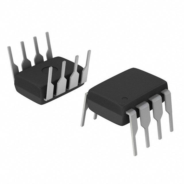
The TLV2472IP is a high-performance CMOS operational amplifier designed for a wide range of applications. Manufactured by Texas Instruments, this dual-channel amplifier is housed in an 8-pin DIP package, making it suitable for through-hole mounting. The TLV2472IP features a supply voltage range of 2.7 V to 6 V, offering flexibility in power supply options. Its gain bandwidth product of 2.8 MHz ensures high-frequency performance, while the slew rate of 1.5 V/µs allows for fast signal transitions. The amplifier is designed to operate with a low supply current of 600 µA across both channels, making it energy-efficient. The input bias current is as low as 2.5 pA, which minimizes the loading effect on the signal source. The voltage input offset is a mere 250 µV, ensuring high accuracy in signal processing. With a maximum output current of 35 mA per channel, the TLV2472IP can drive a variety of loads effectively.
TLV2472IP Features
- Low Power Consumption: The TLV2472IP operates with a supply current of 600 µA (x2 channels), making it suitable for battery-powered and energy-sensitive applications.
- Wide Supply Voltage Range: With a supply voltage span from 2.7 V to 6 V, the TLV2472IP can be used in systems with varying power supply requirements.
- High Gain Bandwidth Product: The 2.8 MHz gain bandwidth product ensures that the amplifier can handle high-frequency signals with minimal distortion.
- Fast Slew Rate: The 1.5 V/µs slew rate allows for rapid signal transitions, making the TLV2472IP ideal for applications requiring fast response times.
- Low Input Bias Current: The 2.5 pA input bias current minimizes the loading effect on the signal source, ensuring high input impedance and accurate signal processing.
- Low Input Offset Voltage: The 250 µV input offset voltage ensures high accuracy and linearity in signal amplification.
- High Output Current: The ability to source or sink up to 35 mA per channel allows the TLV2472IP to drive a variety of loads, including capacitive and resistive loads.
- Compliance and Safety: The TLV2472IP is REACH unaffected and RoHS3 compliant, ensuring environmental safety and regulatory compliance.
TLV2472IP Applications
The TLV2472IP is well-suited for a variety of applications due to its versatile performance characteristics. Some specific use cases include:
- Signal Conditioning: The low input bias current and low input offset voltage make the TLV2472IP ideal for precision signal conditioning in sensor interfaces and analog signal processing.
- Audio Amplification: The high gain bandwidth product and fast slew rate ensure high-fidelity audio amplification, making it suitable for audio equipment.
- Battery-Powered Devices: The low power consumption and wide supply voltage range make the TLV2472IP suitable for portable and battery-powered devices where energy efficiency is crucial.
- Medical Equipment: The high accuracy and low noise characteristics make the TLV2472IP suitable for medical devices that require precise signal processing.
- Automotive Electronics: The robust performance and compliance with environmental standards make the TLV2472IP suitable for automotive applications where reliability and safety are paramount.
Conclusion of TLV2472IP
The TLV2472IP from Texas Instruments is a versatile and high-performance CMOS operational amplifier that offers a combination of low power consumption, wide supply voltage range, high gain bandwidth product, and fast slew rate. Its low input bias current and low input offset voltage ensure high accuracy and precision in signal processing. The TLV2472IP is suitable for a wide range of applications, including signal conditioning, audio amplification, battery-powered devices, medical equipment, and automotive electronics. With its compliance to environmental and safety standards, the TLV2472IP is a reliable choice for modern electronic designs.
Tech Specifications
TLV2472IP Documents
Download datasheets and manufacturer documentation for TLV2472IP
Assembly/Wafer Fab Site 31/Jul/2023 TLV2470-75, TLV247xA Material Set 30/Mar/2017 Related Parts


Shopping Guide


.png?x-oss-process=image/format,webp/resize,h_32)


©2025 ERSA Electronics Corporation.