
Texas Instruments
TLV2632IDR
OP Amps, Buffer Amps ICs


.png?x-oss-process=image/format,webp/resize,p_30)


TLV2632IDR Description
TLV2632IDR Description
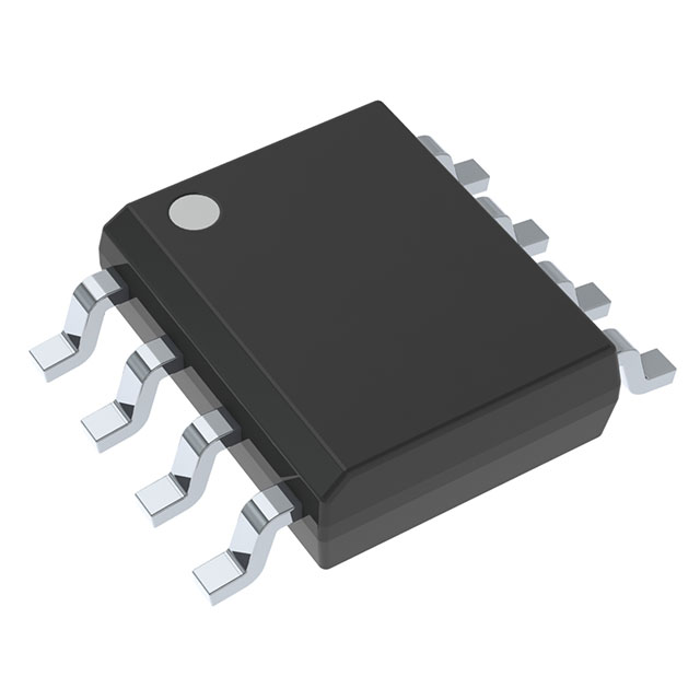
The TLV2632IDR is a high-performance, general-purpose operational amplifier (op-amp) from Texas Instruments, designed for a wide range of applications requiring precision and reliability. This dual-channel op-amp is housed in an 8-pin SOIC package, making it suitable for surface-mount applications. It operates over a wide supply voltage range, from 2.7 V to 5.5 V, ensuring compatibility with various power supply configurations. The TLV2632IDR boasts a gain bandwidth product of 9 MHz and a slew rate of 10 V/µs, providing high-speed performance and excellent signal integrity. With a low input bias current of 0.7 pA and an input offset voltage of 1.1 mV, this op-amp ensures high accuracy and minimal signal distortion. Each channel can source or sink up to 28 mA, making it capable of driving moderate loads. The device is compliant with ROHS3 regulations and is unaffected by REACH, ensuring environmental safety and regulatory compliance.
TLV2632IDR Features
- Wide Supply Voltage Range: Operates from 2.7 V to 5.5 V, offering flexibility in power supply design.
- High Gain Bandwidth Product: 9 MHz ensures high-speed performance, suitable for applications requiring fast signal processing.
- Low Input Bias Current: 0.7 pA minimizes the impact on sensitive input signals, ensuring high accuracy.
- Low Input Offset Voltage: 1.1 mV reduces signal distortion and improves overall system accuracy.
- High Slew Rate: 10 V/µs allows for rapid response to input signal changes, maintaining signal integrity.
- Dual-Channel Design: Two independent op-amp channels provide versatility for multiple signal processing tasks.
- Surface-Mount Compatibility: 8-pin SOIC package is ideal for compact and high-density PCB designs.
- Environmental Compliance: ROHS3 compliant and REACH unaffected, ensuring regulatory compliance and environmental safety.
- Moisture Sensitivity Level: MSL 1 (Unlimited) allows for easy handling and storage without the need for special precautions.
TLV2632IDR Applications
The TLV2632IDR is well-suited for a variety of applications due to its high performance and versatility. Some specific use cases include:
- Signal Conditioning: Ideal for amplifying and conditioning weak signals in sensor interfaces and data acquisition systems.
- Analog Signal Processing: Suitable for applications requiring high-speed signal processing, such as audio and video equipment.
- Power Management: Can be used in power supply circuits for voltage regulation and current sensing.
- Industrial Automation: Provides precision and reliability in control systems and instrumentation.
- Consumer Electronics: Enhances performance in devices such as smartphones, tablets, and home entertainment systems.
Conclusion of TLV2632IDR
The TLV2632IDR from Texas Instruments is a robust and versatile general-purpose op-amp that offers high performance and reliability. Its wide supply voltage range, high gain bandwidth product, and low input bias current make it an excellent choice for a variety of applications. The dual-channel design and surface-mount compatibility further enhance its versatility, making it suitable for both compact and high-density PCB designs. With its environmental compliance and moisture sensitivity level, the TLV2632IDR ensures ease of handling and regulatory compliance. Overall, the TLV2632IDR is an ideal solution for engineers seeking a high-performance op-amp for precision signal processing and conditioning tasks.
Tech Specifications
TLV2632IDR Documents
Download datasheets and manufacturer documentation for TLV2632IDR
 TLV2630-35
  Mult Dev EOL 7/Sep/2023
  Mult Devices Font 21/Apr/2018 Design 25/Feb/2022
 Shopping Guide


.png?x-oss-process=image/format,webp/resize,h_32)


