
 German
 Japanese
 Portuguese
 Korea
Korea
 Mexico
 Dutch
Dutch


Texas Instruments
TLV2633IDGSR

Why Choose Us?
Professional Platform
B2B & B2C purchasingDelivery at full speed
1-2 days deliveryWide variety
Original manufacturers365 days guarantee
Responsible quality
.png)


Tech Specifications
TLV2633IDGSR Description
TLV2633IDGSR Description
The TLV2633IDGSR is a high-performance, general-purpose operational amplifier (op-amp) from Texas Instruments, designed for a wide range of applications requiring precision and reliability. This dual-channel op-amp features a broad supply voltage range, from a minimum of 2.7 V to a maximum of 5.5 V, making it suitable for both low-power and higher voltage applications. The TLV2633IDGSR offers a gain bandwidth product of 9 MHz, ensuring high-frequency performance and stability. With a low input bias current of 0.7 pA, this op-amp minimizes offset errors in sensitive circuits. The device also boasts a fast slew rate of 10 V/µs, which is crucial for applications requiring rapid signal transitions.
TLV2633IDGSR Features
- Wide Supply Voltage Range: Operates from 2.7 V to 5.5 V, providing flexibility in power supply design.
- High Gain Bandwidth Product: 9 MHz ensures excellent performance in high-frequency applications.
- Low Input Bias Current: 0.7 pA reduces offset errors and enhances precision in sensitive circuits.
- Fast Slew Rate: 10 V/µs allows for rapid signal transitions, ideal for high-speed applications.
- Low Supply Current: 3.8 mA per channel ensures efficient power usage, making it suitable for battery-powered devices.
- Low Input Offset Voltage: 1.1 mV ensures high accuracy and precision in signal processing.
- High Output Current: 28 mA per channel supports driving heavy loads without degradation in performance.
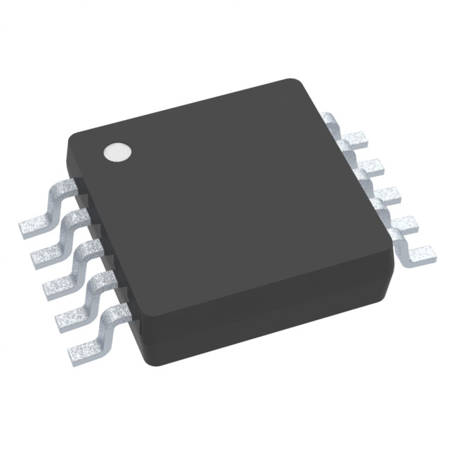
- Surface Mount Package: The 10-pin VSSOP package is compact and suitable for space-constrained designs.
- Compliance and Reliability: ROHS3 compliant and REACH unaffected, ensuring environmental and regulatory compliance.
- Moisture Sensitivity Level (MSL): MSL 1 (Unlimited) ensures robustness in various environmental conditions.
TLV2633IDGSR Applications
The TLV2633IDGSR is ideal for a variety of applications due to its versatile performance characteristics:
- Signal Conditioning: Ideal for amplifying and conditioning weak signals in sensors and transducers.
- Analog Filters: Its high gain bandwidth product makes it suitable for designing active filters with sharp cutoff characteristics.
- Precision Amplification: Low input bias current and low input offset voltage ensure high precision in amplification circuits.
- Consumer Electronics: Suitable for portable devices where low power consumption and compact size are critical.
- Industrial Control: Robust performance and compliance with environmental standards make it suitable for industrial applications.
- Medical Devices: High precision and reliability are essential in medical instrumentation and diagnostic equipment.
Conclusion of TLV2633IDGSR
The TLV2633IDGSR from Texas Instruments is a versatile and high-performance general-purpose op-amp that offers a combination of wide supply voltage range, high gain bandwidth, low input bias current, and fast slew rate. These features make it an excellent choice for a wide range of applications, from signal conditioning to precision amplification. Its compact surface mount package, low power consumption, and compliance with environmental standards further enhance its suitability for modern electronic designs. Whether in consumer electronics, industrial control, or medical devices, the TLV2633IDGSR delivers reliable performance and precision, making it a standout choice in the market.
FAQ
Not available to buy online? Want the lower wholesale price? Please Send RFQ to get best price, we will respond immediately


.png?x-oss-process=image/format,webp/resize,h_32)


