
Texas Instruments
TLV2771IDR
OP Amps, Buffer Amps ICs


.png?x-oss-process=image/format,webp/resize,p_30)


TLV2771IDR Description
TLV2771IDR Description
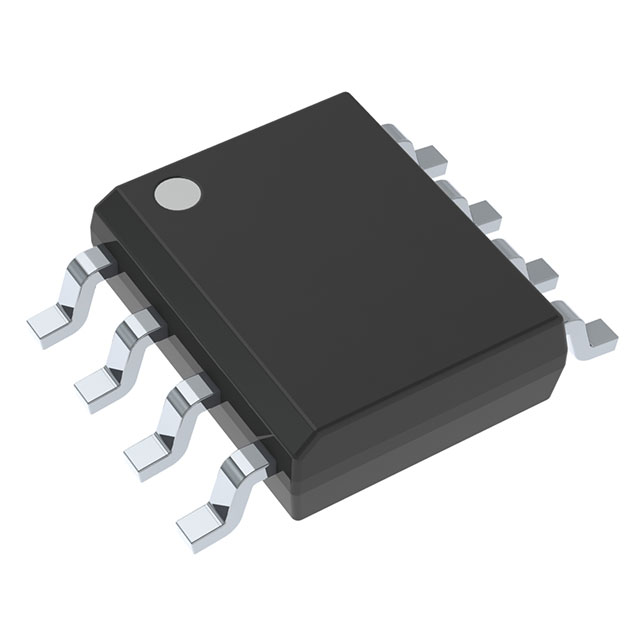
The TLV2771IDR is a general-purpose operational amplifier (op-amp) designed by Texas Instruments, featuring a robust set of specifications suitable for a wide range of applications. This op-amp is housed in an 8-pin SOIC package, making it ideal for surface-mount applications. The TLV2771IDR operates with a supply voltage range of 2.5 V to 5.5 V, ensuring compatibility with various power supply configurations. Its gain bandwidth product of 5.1 MHz and a slew rate of 10.5 V/µs provide high performance in signal processing tasks. The device also boasts a low input bias current of 2 pA and an input offset voltage of 500 µV, ensuring precision in low-level signal amplification.
TLV2771IDR Features
- Wide Supply Voltage Range: The TLV2771IDR operates efficiently within a supply voltage span of 2.5 V to 5.5 V, making it suitable for both low-power and standard voltage applications.
- High Gain Bandwidth Product: With a gain bandwidth product of 5.1 MHz, the TLV2771IDR can handle high-frequency signals with minimal distortion, ensuring accurate amplification across a broad spectrum.
- Low Input Bias Current: The low input bias current of 2 pA minimizes the loading effect on the input signal source, preserving signal integrity and reducing noise.
- High Slew Rate: The 10.5 V/µs slew rate enables the TLV2771IDR to handle fast-changing signals effectively, making it suitable for applications requiring rapid response times.
- Low Input Offset Voltage: The 500 µV input offset voltage ensures high precision in low-level signal amplification, making the TLV2771IDR ideal for sensitive measurement applications.
- Compliance and Packaging: The TLV2771IDR is REACH unaffected and RoHS3 compliant, ensuring environmental sustainability. It is packaged in a tape & reel format, facilitating easy handling and integration into automated assembly processes.
TLV2771IDR Applications
The TLV2771IDR is versatile and can be utilized in a variety of applications due to its general-purpose nature and robust performance characteristics. Some specific use cases include:
- Signal Conditioning: Ideal for amplifying and conditioning weak signals in sensors and transducers, ensuring accurate and reliable data transmission.
- Analog-to-Digital Conversion: Enhances the performance of ADCs by providing a stable and precise signal, improving overall system accuracy.
- Active Filters: Can be used in designing active filters for various frequency ranges, thanks to its high gain bandwidth product and low input offset voltage.
- Precision Amplification: Suitable for applications requiring high-precision amplification, such as medical equipment and scientific instruments.
- Consumer Electronics: Ideal for use in consumer electronics where low power consumption and high performance are critical.
Conclusion of TLV2771IDR
The TLV2771IDR from Texas Instruments stands out as a reliable and high-performance general-purpose op-amp. Its wide supply voltage range, high gain bandwidth product, low input bias current, and high slew rate make it suitable for a broad range of applications. The TLV2771IDR’s compliance with environmental standards and its surface-mount package further enhance its appeal for modern electronics design. Whether used in signal conditioning, precision amplification, or active filters, the TLV2771IDR delivers consistent performance and reliability, making it a valuable component in any electronics engineer’s toolkit.
Tech Specifications
TLV2771IDR Documents
Download datasheets and manufacturer documentation for TLV2771IDR
 Product Discontinuance Notification 2024-04-05 (PDF) Product Discontinuance Notification (PDF)
  Mechanical Outline Drawing
  TLV277x/TLV277xA EMI Immunity Performance Signal Conditioning Piezoelectric Sensors (Rev. A)
  TLV277xA PSpice 5V Supply Voltage Model
 Shopping Guide


.png?x-oss-process=image/format,webp/resize,h_32)


