
 German
 Japanese
 Portuguese
 Korea
Korea
 Mexico
 Dutch
Dutch


Texas Instruments
TLV2772QPW

Why Choose Us?
Professional Platform
B2B & B2C purchasingDelivery at full speed
1-2 days deliveryWide variety
Original manufacturers365 days guarantee
Responsible quality
.png)


Tech Specifications
TLV2772QPW Description
TLV2772QPW Description
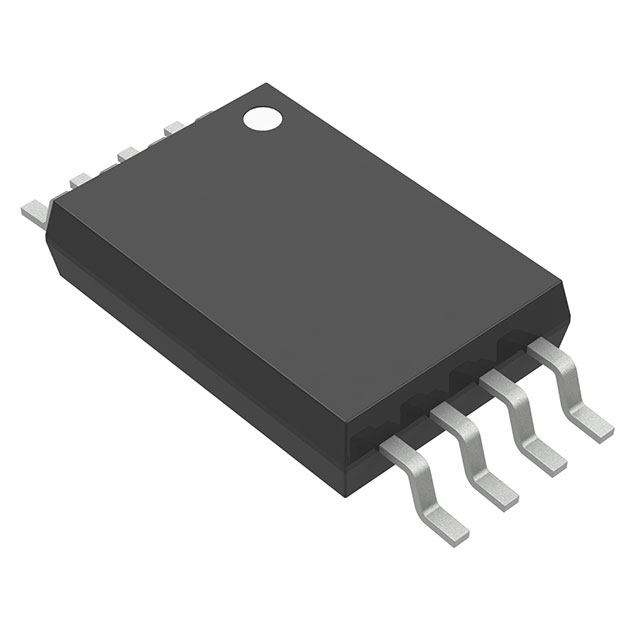
The TLV2772QPW from Texas Instruments is a high-performance, automotive-grade CMOS operational amplifier designed for precision applications. Housed in an 8-TSSOP package, this dual-channel op-amp operates over a 2.5V to 5.5V supply range, making it suitable for low-voltage systems. With a 5.1 MHz gain bandwidth product (GBW) and 10.5V/µs slew rate, it delivers fast signal processing while maintaining low power consumption (1mA per channel). Its ultra-low input bias current (2 pA) and 360 µV input offset voltage ensure high accuracy in sensitive circuits. The device is ROHS3 compliant and REACH unaffected, meeting stringent environmental and automotive standards.
TLV2772QPW Features
- Automotive-Grade: Qualified for harsh environments, ensuring reliability in automotive applications.
- Low Power, High Speed: Optimized for 5.1 MHz GBW and 10.5V/µs slew rate at just 1mA/channel supply current.
- Precision Performance: 2 pA input bias current and 360 µV offset voltage for high-accuracy signal conditioning.
- Wide Supply Range: Operates from 2.5V to 5.5V, ideal for battery-powered and low-voltage systems.
- Robust Packaging: 8-TSSOP surface-mount package with MSL1 (Unlimited) moisture sensitivity, suitable for automated assembly.
TLV2772QPW Applications
- Sensor Interfaces: Ideal for amplifying low-level signals from sensors (e.g., temperature, pressure) due to its low noise and high precision.
- Battery-Powered Systems: Efficient operation at low voltages extends battery life in portable devices.
- Active Filters: High GBW and slew rate enable stable performance in filter designs.
- Automotive Electronics: Suitable for ECUs, infotainment, and ADAS due to automotive-grade reliability.
- Signal Conditioning: Excellent for ADC drivers and precision instrumentation.
Conclusion of TLV2772QPW
The TLV2772QPW combines low power, high speed, and precision in a compact, automotive-qualified package. Its wide supply range and ultra-low input bias current make it versatile for sensor interfaces, battery-operated devices, and automotive systems. While it is on Last Time Buy status, its performance advantages over similar CMOS op-amps (e.g., lower offset voltage, higher slew rate) ensure it remains a compelling choice for critical designs requiring reliability and accuracy. Engineers should consider this IC for applications demanding low-voltage operation with minimal error.
FAQ
Not available to buy online? Want the lower wholesale price? Please Send RFQ to get best price, we will respond immediately


.png?x-oss-process=image/format,webp/resize,h_32)


