
 German
 Japanese
 Portuguese
 Korea
Korea
 Mexico
 Dutch
Dutch


Texas Instruments
TLV342IDGKR

Why Choose Us?
Professional Platform
B2B & B2C purchasingDelivery at full speed
1-2 days deliveryWide variety
Original manufacturers365 days guarantee
Responsible quality
.png)


Tech Specifications
TLV342IDGKR Description
TLV342IDGKR Description
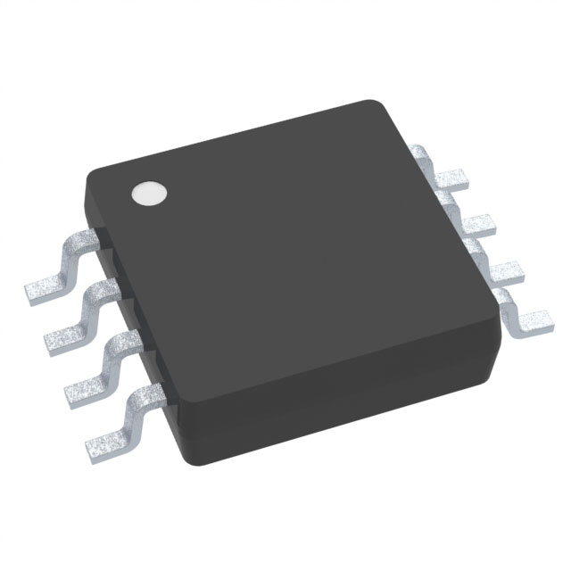
The TLV342IDGKR is a CMOS operational amplifier (op-amp) from Texas Instruments, designed for high performance in a wide range of applications. It features a dual-channel configuration, allowing for more efficient use of space and power in systems requiring multiple op-amps. The device is housed in an 8-pin very small shunt outline (VSSOP) package, making it suitable for surface-mount applications.
TLV342IDGKR Features
- Voltage Supply Span: The TLV342IDGKR operates over a wide voltage range, from 1.5 V to 5.5 V, providing flexibility in power supply design.
- Gain Bandwidth Product: With a gain bandwidth product of 2.3 MHz, the op-amp offers high-speed performance for demanding applications.
- Slew Rate: The device boasts a slew rate of 1 V/µs, enabling rapid response to input changes.
- Input Bias Current: The ultra-low input bias current of 1 pA minimizes input offset voltage drift and power consumption.
- Supply Current: The TLV342IDGKR consumes only 75 µA per channel, making it energy-efficient.
- Input Offset Voltage: A low input offset voltage of 300 µV ensures high accuracy in signal amplification.
- Output Current: Each channel can provide up to 115 mA, suitable for driving capacitive loads.
- Mounting Type: Surface-mount technology allows for compact and reliable integration into printed circuit boards.
- Package: The device is available in tape and reel packaging, facilitating automated assembly processes.
- Compliance: The TLV342IDGKR is compliant with RoHS3 standards, making it suitable for environmentally conscious designs.
TLV342IDGKR Applications
The TLV342IDGKR is ideal for a variety of applications where high performance, low power consumption, and space efficiency are critical:
- Audio Amplification: The low noise and high slew rate make it suitable for audio signal processing.
- Sensor Conditioning: The low input bias current and low offset voltage are beneficial for accurate sensor signal conditioning.
- Data Acquisition Systems: The wide supply voltage range and low power consumption make it ideal for battery-operated data acquisition systems.
- Industrial Control: The device's robust performance and compliance with RoHS3 standards make it suitable for industrial control applications.
Conclusion of TLV342IDGKR
The TLV342IDGKR is a versatile CMOS op-amp that combines high performance with low power consumption and space efficiency. Its unique features, such as the wide voltage supply span, low input bias current, and dual-channel configuration, make it an excellent choice for a variety of applications in audio, sensor conditioning, data acquisition, and industrial control. With its compliance with RoHS3 standards and REACH unaffected status, the TLV342IDGKR is also an environmentally responsible choice for designers looking to meet stringent environmental regulations.
FAQ
| Quantity | Unit Price | Ext. Price |
|---|---|---|
| 1+ | $0.84857 | $0.85 |
| 10+ | $0.82800 | $8.28 |
| 30+ | $0.81428 | $24.43 |
Not available to buy online? Want the lower wholesale price? Please Send RFQ to get best price, we will respond immediately


.png?x-oss-process=image/format,webp/resize,h_32)


