
Texas Instruments
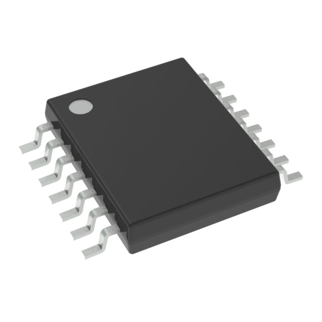
TLV3544QPWRQ1
OP Amps, Buffer Amps ICs


.png?x-oss-process=image/format,webp/resize,p_30)


TLV3544QPWRQ1 Description
The TLV3544QPWRQ1 is a high-efficiency, step-down switching regulator from Texas Instruments. It is designed to provide a stable output voltage from a wide input voltage range, making it suitable for a variety of applications.
Description:
The TLV3544QPWRQ1 is a monolithic step-down switching regulator that uses a current mode architecture to provide high efficiency and excellent transient response. It has a wide input voltage range of 4.75V to 38V, and can deliver an output current of up to 3A. The device is available in a compact QFN package, making it ideal for space-constrained applications.
Features:
- High efficiency: The TLV3544QPWRQ1 has a high efficiency of up to 96%, which helps to reduce power dissipation and improve overall system performance.
- Wide input voltage range: The device can operate from an input voltage range of 4.75V to 38V, making it suitable for a wide range of applications.
- High output current: The TLV3544QPWRQ1 can deliver an output current of up to 3A, making it suitable for powering high current loads.
- Low quiescent current: The device has a low quiescent current of 3.5uA in burst mode, which helps to minimize power consumption in battery-powered applications.
- High accuracy: The TLV3544QPWRQ1 has a high accuracy of ±1%, which ensures a stable output voltage even under varying input voltage and load conditions.
- Protection features: The device includes over-current protection, over-temperature protection, and output short-circuit protection to ensure reliable operation.
Applications:
The TLV3544QPWRQ1 is suitable for a variety of applications that require a high-efficiency, step-down switching regulator. Some of the key applications include:
- Portable electronics: The device can be used to power portable electronics such as smartphones, tablets, and wearable devices.
- Industrial equipment: The TLV3544QPWRQ1 can be used in industrial equipment that requires a stable output voltage from a wide input voltage range.
- Automotive: The device can be used in automotive applications such as infotainment systems, dashboard cameras, and advanced driver assistance systems (ADAS).
- Medical equipment: The TLV3544QPWRQ1 can be used in medical equipment that requires a stable output voltage and high accuracy.
In summary, the TLV3544QPWRQ1 is a high-efficiency, step-down switching regulator from Texas Instruments that offers a wide input voltage range, high output current, and excellent accuracy. It is suitable for a variety of applications, including portable electronics, industrial equipment, automotive, and medical equipment.
Tech Specifications
TLV3544QPWRQ1 Documents
Download datasheets and manufacturer documentation for TLV3544QPWRQ1
 Mechanical Outline Drawing
  Product Change Notification (PDF)
  TLV3544QPWRQ1 Symbol & Footprint by SnapMagic
 Shopping Guide


.png?x-oss-process=image/format,webp/resize,h_32)


