
 German
 Japanese
 Portuguese
 Korea
Korea
 Mexico
 Dutch
Dutch


Texas Instruments
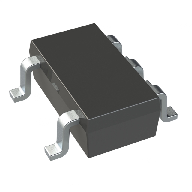
TLV365QDBVRQ1

Why Choose Us?
Professional Platform
B2B & B2C purchasingDelivery at full speed
1-2 days deliveryWide variety
Original manufacturers365 days guarantee
Responsible quality
.png)


Tech Specifications
TLV365QDBVRQ1 Description
TLV365QDBVRQ1 Description
The TLV365QDBVRQ1 is an automotive-grade, single-supply operational amplifier designed for high-performance applications. Manufactured by Texas Instruments, this linear IC chip offers a wide supply voltage range from 2.2 V to 5.5 V, making it suitable for various power supply configurations. The device features a high slew rate of 27 V/µs and a gain bandwidth product of 50 MHz, ensuring excellent performance in high-frequency and fast-switching applications. With a supply current of only 4.6 mA, the TLV365QDBVRQ1 is optimized for low power consumption, making it ideal for energy-efficient designs.
TLV365QDBVRQ1 Features
- Wide Supply Voltage Range: The TLV365QDBVRQ1 operates from 2.2 V to 5.5 V, providing flexibility in power supply requirements.
- High Slew Rate: With a slew rate of 27 V/µs, this op-amp can handle fast signal transitions, making it suitable for high-speed applications.
- High Gain Bandwidth Product: The 50 MHz gain bandwidth product ensures stable performance across a wide frequency range.
- Low Input Bias Current: The low input bias current of 5 pA minimizes offset errors and improves signal integrity.
- Low Input Offset Voltage: The 400 µV input offset voltage ensures accurate signal processing and minimal distortion.
- High Output Current: The device can deliver up to 85 mA per channel, supporting high-current applications.
- Automotive Grade: Certified for automotive applications, the TLV365QDBVRQ1 meets stringent reliability and performance standards.
- Compliance: The TLV365QDBVRQ1 is REACH unaffected and RoHS3 compliant, ensuring environmental and safety standards are met.
- Moisture Sensitivity Level: MSL 1 (Unlimited) indicates the device is suitable for surface mount applications without additional moisture protection.
TLV365QDBVRQ1 Applications
The TLV365QDBVRQ1 is ideal for a variety of automotive applications where high performance and reliability are critical. Specific use cases include:
- Automotive Electronics: Ideal for in-vehicle infotainment systems, advanced driver-assistance systems (ADAS), and other electronic control units (ECUs).
- Signal Processing: Suitable for high-speed signal conditioning and processing in sensor interfaces and data acquisition systems.
- Power Management: The low supply current and wide voltage range make it suitable for power management circuits in automotive powertrain and body electronics.
- High-Speed Amplification: The high slew rate and gain bandwidth product make it suitable for applications requiring fast and accurate signal amplification.
Conclusion of TLV365QDBVRQ1
The TLV365QDBVRQ1 from Texas Instruments is a robust and versatile operational amplifier designed for automotive applications. Its wide supply voltage range, high slew rate, and low power consumption make it an excellent choice for high-performance, energy-efficient designs. The device's automotive-grade certification ensures reliability and compliance with industry standards. Whether used in automotive electronics, signal processing, or power management, the TLV365QDBVRQ1 offers superior performance and reliability, making it a standout choice in its category.
FAQ
Not available to buy online? Want the lower wholesale price? Please Send RFQ to get best price, we will respond immediately


.png?x-oss-process=image/format,webp/resize,h_32)


