
Texas Instruments
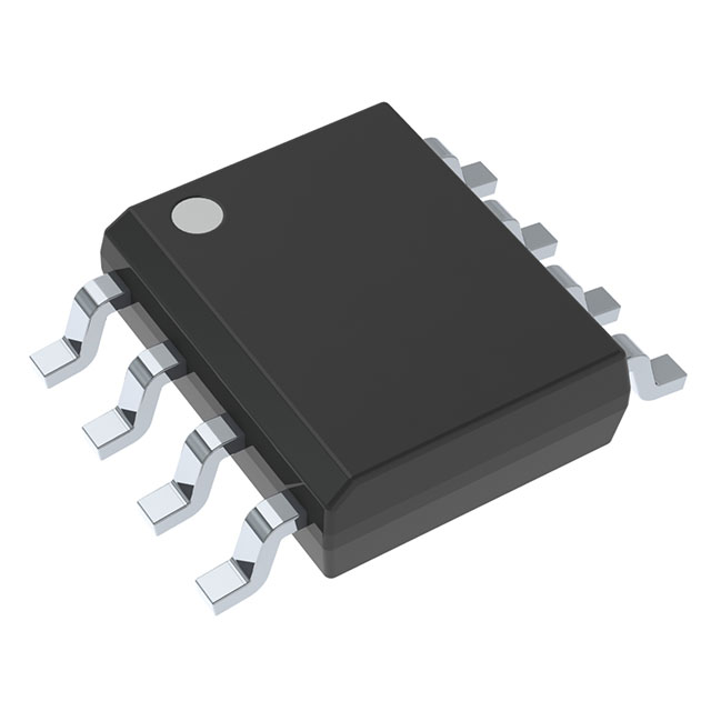
TLV4110IDG4
OP Amps, Buffer Amps ICs


.png?x-oss-process=image/format,webp/resize,p_30)


TLV4110IDG4 Description
TLV4110IDG4 Description
The TLV4110IDG4 is a high-performance general-purpose operational amplifier (op-amp) designed by Texas Instruments. This op-amp is ideal for a wide range of applications due to its robust performance and versatile specifications. With a supply voltage range of 2.5 V to 6 V, it offers flexibility in power supply options, making it suitable for both low-voltage and standard voltage systems. The TLV4110IDG4 features a gain bandwidth product of 2.7 MHz, ensuring high-frequency performance and stability in various electronic circuits.
TLV4110IDG4 Features
- Low Input Bias Current: The TLV4110IDG4 boasts an impressively low input bias current of 0.3 pA, which minimizes the effect of input currents on the circuit, especially in high-impedance applications.
- High Slew Rate: With a slew rate of 1.57 V/µs, this op-amp can handle high-frequency signals effectively, making it suitable for applications requiring fast transient response.
- Low Input Offset Voltage: The voltage input offset is as low as 175 µV, ensuring high accuracy and precision in signal processing.
- Low Supply Current: The op-amp operates with a supply current of only 700 µA, making it energy-efficient and suitable for battery-powered and low-power applications.
- High Output Current Capability: The TLV4110IDG4 can deliver up to 320 mA of output current per channel, providing robust performance for driving various loads.
- Surface Mount Technology: The surface mount package type ensures ease of integration into modern PCB designs, facilitating compact and reliable electronic systems.
- Compliance and Reliability: The TLV4110IDG4 is REACH unaffected and RoHS3 compliant, ensuring environmental safety and regulatory compliance. It also has a moisture sensitivity level (MSL) of 1, making it suitable for a wide range of manufacturing environments.
TLV4110IDG4 Applications
The TLV4110IDG4 is well-suited for a variety of applications due to its versatile performance characteristics. Some specific use cases include:
- Signal Conditioning: Ideal for amplifying and conditioning weak signals in sensors and transducers, ensuring high accuracy and reliability in signal transmission.
- Audio Applications: Its high slew rate and low input bias current make it suitable for audio amplifiers, where high-fidelity signal reproduction is crucial.
- Low-Power Systems: The low supply current and wide supply voltage range make it an excellent choice for battery-operated devices and portable electronics.
- Industrial Control Systems: The op-amp's robust performance and high output current capability make it suitable for driving actuators and controlling processes in industrial environments.
- Medical Devices: Its low input offset voltage and high precision make it ideal for medical instrumentation where accuracy and reliability are paramount.
Conclusion of TLV4110IDG4
The TLV4110IDG4 from Texas Instruments stands out as a versatile and high-performance general-purpose op-amp. Its low input bias current, high slew rate, and low input offset voltage make it suitable for a wide range of applications, from precision signal processing to high-frequency amplification. The op-amp's low supply current and wide supply voltage range further enhance its adaptability, making it an excellent choice for both low-power and standard voltage systems. With its surface mount package and compliance with environmental regulations, the TLV4110IDG4 ensures ease of integration and reliability in modern electronic designs.
Tech Specifications
TLV4110IDG4 Documents
Download datasheets and manufacturer documentation for TLV4110IDG4
 TLV4110-13
  TLV4110-13
 Shopping Guide


.png?x-oss-process=image/format,webp/resize,h_32)


