
 German
 Japanese
 Portuguese
 Korea
Korea
 Mexico
 Dutch
Dutch


Texas Instruments
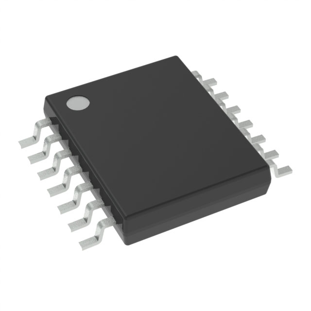
TLV4197QPWRQ1

Why Choose Us?
Professional Platform
B2B & B2C purchasingDelivery at full speed
1-2 days deliveryWide variety
Original manufacturers365 days guarantee
Responsible quality
.png)


Tech Specifications
TLV4197QPWRQ1 Description
Description:
The TLV4197QPWRQ1 is a high-precision, low-power operational amplifier (op-amp) manufactured by Texas Instruments. This device is designed to provide excellent performance in a wide range of applications, including precision measurement, sensor conditioning, and signal processing. The TLV4197QPWRQ1 is available in a small, 8-pin QFN package, making it suitable for space-constrained applications.
Features:
- High precision: The TLV4197QPWRQ1 offers excellent precision with a maximum input offset voltage of 1 µV and a maximum input offset voltage drift of 0.2 µV/°C.
- Low power consumption: The device operates with a low supply current of 95 µA, making it suitable for battery-powered applications.
- Wide supply voltage range: The TLV4197QPWRQ1 can operate with a supply voltage range of 2.7 V to 5.5 V, providing flexibility in system design.
- Low input bias current: The device has a low input bias current of 1 pA, which is beneficial for applications involving high-impedance inputs.
- High output drive capability: The TLV4197QPWRQ1 can drive capacitive loads up to 10 pF, making it suitable for driving high-speed loads.
- Rail-to-rail input and output: The op-amp can operate with input signals that go all the way to the supply rails, and it also provides rail-to-rail output swing, ensuring maximum utilization of the supply voltage.
- Internal frequency compensation: The TLV4197QPWRQ1 includes internal frequency compensation, eliminating the need for external components for stability.
Applications:
- Precision measurement: The high precision and low drift of the TLV4197QPWRQ1 make it suitable for applications such as pressure sensors, temperature sensors, and strain gauges.
- Medical instrumentation: The device's low noise and high precision make it ideal for medical equipment, such as blood pressure monitors and other diagnostic devices.
- Industrial control systems: The TLV4197QPWRQ1 can be used in industrial control systems for signal conditioning and processing, where accurate measurements are critical.
- Battery-powered devices: The low power consumption of the op-amp makes it suitable for battery-powered applications, such as portable data acquisition systems and wireless sensors.
- Audio equipment: The TLV4197QPWRQ1 can be used in audio equipment for precise signal processing and amplification, providing high-quality sound reproduction.
- Data converters: The device can be used in conjunction with data converters (ADCs and DACs) for high-precision signal conditioning and amplification.
- Energy harvesting systems: The low power consumption of the TLV4197QPWRQ1 makes it suitable for energy harvesting applications, where power management is crucial.
In summary, the TLV4197QPWRQ1 is a high-precision, low-power operational amplifier from Texas Instruments, suitable for a wide range of applications, including precision measurement, sensor conditioning, and signal processing. Its features, such as low input offset voltage, low power consumption, and rail-to-rail input and output, make it an excellent choice for various applications where precision and low power are critical.
FAQ
Not available to buy online? Want the lower wholesale price? Please Send RFQ to get best price, we will respond immediately


.png?x-oss-process=image/format,webp/resize,h_32)


