
 German
 Japanese
 Portuguese
 Korea
Korea
 Mexico
 Dutch
Dutch


Texas Instruments
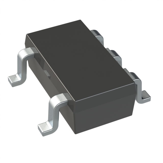
TLV7011DBVR

Why Choose Us?
Professional Platform
B2B & B2C purchasingDelivery at full speed
1-2 days deliveryWide variety
Original manufacturers365 days guarantee
Responsible quality
.png)


Tech Specifications
TLV7011DBVR Description
The TLV7011DBVR is a low-dropout (LDO) linear voltage regulator manufactured by Texas Instruments. This LDO regulator is designed to provide a stable and reliable output voltage to power various electronic devices and systems.
Description:
The TLV7011DBVR is a compact, low-power LDO regulator available in a small SOT-23 package. It has a wide input voltage range of 1.9V to 5.5V and can deliver an output current of up to 300mA. The device features a low dropout voltage of typically 250mV at 300mA output current, ensuring efficient power delivery even under low-voltage conditions.
Features:
- Wide input voltage range: 1.9V to 5.5V
- Output current capability: Up to 300mA
- Low dropout voltage: Typically 250mV at 300mA output current
- Low quiescent current: 5.5µA (typical)
- Small package size: SOT-23
- Internal current limit and thermal shutdown protection
- Low output voltage drift: 1% maximum over temperature and line
- Enable function with active low input
- Fixed output voltage options available: 1.8V, 2.5V, 2.85V, 3.3V, and adjustable output version
Applications:
The TLV7011DBVR is suitable for a wide range of applications where a stable and efficient power supply is required. Some common applications include:
- Portable and battery-powered devices: Mobile phones, tablets, and wearable electronics
- IoT devices: Sensors, smart home devices, and wireless communication modules
- Industrial equipment: Control systems, monitoring devices, and automation equipment
- Medical devices: Patient monitoring systems, portable medical instruments, and wearable medical devices
- Consumer electronics: Audio equipment, GPS devices, and digital cameras
- Automotive electronics: Infotainment systems, sensor interfaces, and control modules
The TLV7011DBVR's low dropout voltage, low quiescent current, and small package size make it an ideal choice for applications where space and power efficiency are critical.
FAQ
| Quantity | Unit Price | Ext. Price |
|---|---|---|
| 10+ | $0.39600 | $3.96 |
| 30+ | $0.34457 | $10.34 |
| 100+ | $0.30343 | $30.34 |
| 500+ | $0.28972 | $144.86 |
| 1000+ | $0.28285 | $282.85 |
Not available to buy online? Want the lower wholesale price? Please Send RFQ to get best price, we will respond immediately


.png?x-oss-process=image/format,webp/resize,h_32)


