Texas Instruments_TLV70229QDSERQ1

Texas Instruments
TLV70229QDSERQ1  
Linear & Switching Voltage Regulators

Texas Instruments
TLV70229QDSERQ1
776-TLV70229QDSERQ1
Ersa
Texas Instruments-TLV70229QDSERQ1-datasheets-10158323.pdf
IC REG LINEAR 2.9V 300MA 6WSON
In Stock : 9005

Not available to buy online? Want the lower wholesale price? Please Send RFQ to get best price, we will respond immediately

QUICK RFQ
ADD TO RFQ LIST
ersa FreeSample ersa flow
  • Quantity
  • Unit Price
  • Ext. Price
    • 1+
    • $0.28483
    • $0.28
    • 10+
    • $0.24674
    • $2.47
    • 30+
    • $0.20717
    • $6.22
    • 100+
    • $0.18779
    • $18.78
    • 500+
    • $0.18034
    • $90.17
    • 1000+
    • $0.17438
    • $174.38
    ADD TO CART
    QUICK ORDER
    $0.28483    $0.28
    ISO9001
    Quality Policy
    ISO45001
    ISO14001

    TLV70229QDSERQ1 Description

    The TLV70229QDSERQ1 is a low-dropout (LDO) linear voltage regulator manufactured by Texas Instruments. This device is designed to provide a stable and reliable voltage output for a wide range of applications.

    Description:

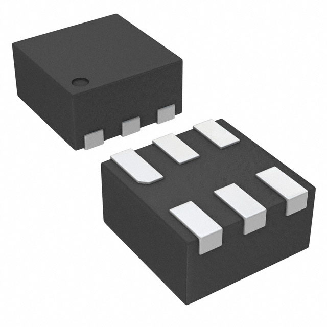
    The TLV70229QDSERQ1 is a low-dropout linear voltage regulator with an input voltage range of 2.5V to 5.5V and an output voltage range of 1.23V to 3.3V. It features a very low dropout voltage of 180mV at maximum load, which ensures stable output voltage even when the input voltage is close to the output voltage. The device is available in a small, thermally enhanced QFN package.

    Features:

    1. Ultra-low dropout voltage of 180mV at maximum load
    2. Wide input voltage range of 2.5V to 5.5V
    3. Wide output voltage range of 1.23V to 3.3V
    4. High output current capability of up to 2A
    5. Low quiescent current of 65µA (typical)
    6. Small thermally enhanced QFN package
    7. Internal current limit and thermal shutdown protection
    8. Low output noise and high PSRR (Power Supply Reject Ratio)

    Applications:

    The TLV70229QDSERQ1 is suitable for a wide range of applications that require a stable and reliable voltage source. Some of the common applications include:

    1. Portable devices: Smartphones, tablets, and wearable devices
    2. IoT devices: Sensors, smart home devices, and IoT gateways
    3. Industrial equipment: Control systems, motor drivers, and industrial communication devices
    4. Medical equipment: Patient monitoring devices, medical imaging equipment, and portable medical devices
    5. Automotive applications: Infotainment systems, sensor interfaces, and power management systems

    The TLV70229QDSERQ1's low dropout voltage, wide input and output voltage range, and high output current capability make it an ideal choice for applications that require a stable and efficient voltage regulator in a compact form factor.

    Tech Specifications

    Unit Weight
    Product
    Voltage Regulation Accuracy
    PPAP
    Automotive
    Special Features
    RoHS
    Line Regulation
    PSRR / Ripple Rejection - Typ
    Thermal resistance θJA (°C/W)
    Maximum Input Voltage (V)
    REACH Status
    Accuracy (%)
    Operating temperature range (°C)
    Vout (min) (V)
    Maximum Output Current (A)
    Supplier Temperature Grade
    Vin (min) (V)
    Standard Package Name
    Mounting
    Qualification
    Fixed output options (V)
    Package
    Load Regulation
    PSRR at 100 KHz (dB)
    Output Type
    Iq (typ) (mA)
    Development Kit
    Package Height
    Maximum Operating Temperature
    Voltage Dropout (Max)
    RoHS Status
    Load capacitance (min) (µF)
    Junction to Ambient
    Voltage - Output (Max)
    Minimum Operating Temperature
    Type
    Part Status
    Lead finish / Ball material
    Package Width
    Output Voltage Range
    Output options
    Number of Regulators
    Dropout voltage (Vdo) (typ) (mV)
    Product Status
    Supplier Package
    Junction to Case
    Package / Case
    Vout (max) (V)
    Maximum Dropout Voltage @ Current (V)
    EU RoHS
    Carrier
    Vin (max) (V)
    Dropout Voltage
    Moisture Sensitivity Level (MSL)
    Operating Temperature
    PSRR
    Output Current
    ECCN
    Grade
    MSL rating / Peak reflow
    Mounting Type
    Pin Count
    Control Features
    Lead Shape
    Quiescent Current
    Output Voltage (V)
    HTSUS
    Pins
    USHTS
    Output Voltage
    Typical Ground Current @ Full Load (mA)
    Minimum Input Voltage (V)
    PCB changed
    Dropout Voltage - Max
    Voltage - Input (Max)
    HTS
    Rating
    Current - Output
    ECCN (US)
    Output Configuration
    Current - Supply (Max)
    Input Voltage - Max
    Supplier Device Package
    Minimum Operating Temperature (°C)
    Maximum Operating Temperature (°C)
    Input Voltage - Min
    Mfr
    Voltage - Output (Min/Fixed)
    Polarity
    Features
    Mounting Style
    Regulated outputs (#)
    Current - Quiescent (Iq)
    Package Length
    Number of Outputs
    REACH
    Iout (max) (A)
    Series
    Protection Features
    Base Product Number
    Noise (µVrms)

    TLV70229QDSERQ1 Documents

    Download datasheets and manufacturer documentation for TLV70229QDSERQ1

    Ersa Wafer Fab/Test Site 23/May/2023      
    Ersa TLV702-Q1 Datasheet      
    Ersa TLV702-Q1 Datasheet      
    Ersa TLV702 Datasheet Chg 27/Aug/2019      

    Shopping Guide

    Payment Methods
    Payment Methods include Prepayment TT (bank transfer), Western Union, and PayPal. Customers are responsible for shipping costs, bank charges, customs duties and taxes.
    Shipping Rate
    Shipments are made once a day around 5pm, excluding Sundays. Once shipped, the estimated delivery time is usually 5-7 business days, depending on the courier you choose.
    Delivery Methods
    Provide DHL, FedEx, UPS, EMS, SF Express and Registered Airmail International Delivery Service