
 German
 Japanese
 Portuguese
 Korea
Korea
 Mexico
 Dutch
Dutch


Texas Instruments
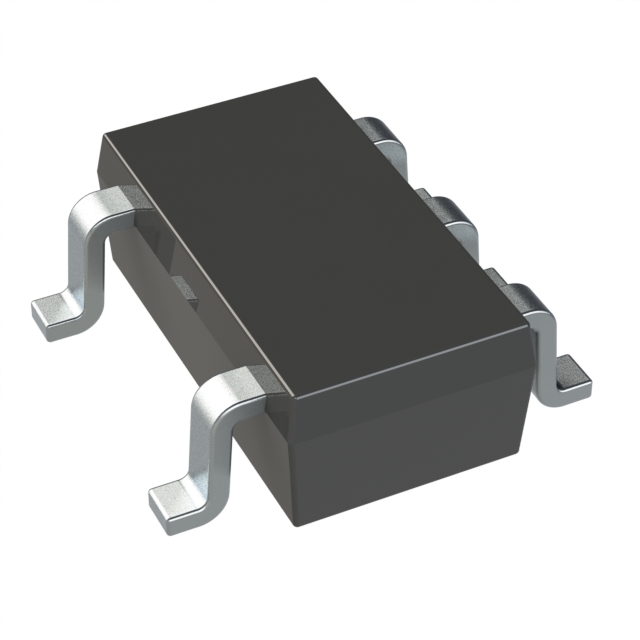
TLV9001UIDBVR

Why Choose Us?
Professional Platform
B2B & B2C purchasingDelivery at full speed
1-2 days deliveryWide variety
Original manufacturers365 days guarantee
Responsible quality
.png)


Tech Specifications
TLV9001UIDBVR Description
TLV9001UIDBVR Description
The TLV9001UIDBVR is a high-performance operational amplifier (op-amp) from Texas Instruments, designed to deliver exceptional performance in a compact SOT23-5 package. With a maximum supply voltage of 5.5 V and a minimum supply voltage of 1.8 V, this CMOS op-amp offers a wide operating voltage range, making it suitable for various applications. The TLV9001UIDBVR boasts a gain bandwidth product of 1 MHz and a slew rate of 2V/µs, ensuring fast response times and high-frequency performance.
TLV9001UIDBVR Features
- Wide Supply Voltage Range: The TLV9001UIDBVR operates over a supply voltage range of 1.8 V to 5.5 V, providing flexibility in power supply design.
- High Gain Bandwidth Product: With a gain bandwidth product of 1 MHz, this op-amp is capable of handling high-frequency signals with ease.
- Fast Slew Rate: The 2V/µs slew rate ensures quick response times and minimal distortion in high-speed applications.
- Low Input Bias Current: The 5 pA input bias current minimizes power consumption and reduces noise in sensitive circuits.
- Low Input Offset Voltage: The 400 µV input offset voltage ensures accurate signal amplification and low distortion.
- Low Supply Current: The 60 µA supply current makes the TLV9001UIDBVR ideal for battery-powered applications.
- High Output Current: The 40 mA output current per channel allows for driving demanding loads.
- RoHS Compliance: The TLV9001UIDBVR is compliant with RoHS3 standards, making it suitable for environmentally conscious designs.
- REACH Unaffected: This op-amp is not affected by REACH regulations, ensuring uninterrupted supply and compliance with European chemical regulations.
TLV9001UIDBVR Applications
The TLV9001UIDBVR is an ideal choice for a wide range of applications due to its high performance and compact form factor. Some specific use cases include:
- Audio Amplification: The low noise and high slew rate make it suitable for audio signal amplification in consumer electronics.
- Sensor Signal Conditioning: The low input bias current and low input offset voltage make it ideal for conditioning signals from sensors in industrial and automotive applications.
- Battery-Powered Devices: The low supply current and wide supply voltage range make it suitable for battery-powered devices, such as portable electronics and wearables.
- Data Acquisition Systems: The high gain bandwidth product and fast slew rate make it suitable for amplifying and processing signals in data acquisition systems.
Conclusion of TLV9001UIDBVR
The TLV9001UIDBVR is a versatile and high-performance op-amp from Texas Instruments, offering a wide supply voltage range, high gain bandwidth product, and low input bias current. Its compact SOT23-5 package and RoHS compliance make it an ideal choice for a variety of applications, including audio amplification, sensor signal conditioning, battery-powered devices, and data acquisition systems. With its unique combination of performance and features, the TLV9001UIDBVR stands out as a superior option in the crowded market of op-amps and buffer amplifiers.
FAQ
| Quantity | Unit Price | Ext. Price |
|---|---|---|
| 5+ | $0.33764 | $1.69 |
| 50+ | $0.27173 | $13.59 |
| 150+ | $0.23956 | $35.93 |
| 500+ | $0.21085 | $105.43 |
Not available to buy online? Want the lower wholesale price? Please Send RFQ to get best price, we will respond immediately


.png?x-oss-process=image/format,webp/resize,h_32)


