
 German
 Japanese
 Portuguese
 Korea
Korea
 Mexico
 Dutch
Dutch


Texas Instruments
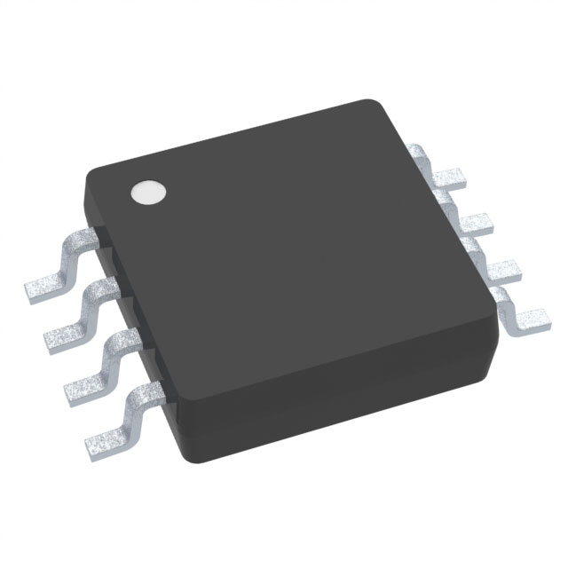
TLV9002IDGKR

Why Choose Us?
Professional Platform
B2B & B2C purchasingDelivery at full speed
1-2 days deliveryWide variety
Original manufacturers365 days guarantee
Responsible quality
.png)


Tech Specifications
TLV9002IDGKR Description
The TLV9002IDGKR is a low-power, single-supply, monolithic integrated circuit from Texas Instruments that is designed for use in a variety of applications, including portable equipment, battery-powered devices, and industrial systems. Here is a description of the TLV9002IDGKR, including its features and applications:
Description:
The TLV9002IDGKR is a low-power, single-supply, monolithic integrated circuit that provides high-quality video performance in a compact package. It is designed to be used in a variety of applications, including portable equipment, battery-powered devices, and industrial systems. The device features a low power consumption of 180mW, making it ideal for use in battery-powered applications.
Features:
- Low power consumption of 180mW
- Single-supply operation
- Monolithic design for compactness
- High-quality video performance
- Wide input voltage range of 2.7V to 5.5V
- Low output voltage noise of 50µV
- Wide operating temperature range of -40°C to +85°C
- RoHS compliant
Applications:
The TLV9002IDGKR is suitable for use in a variety of applications, including:
- Portable equipment
- Battery-powered devices
- Industrial systems
- Video processing systems
- Medical imaging systems
- Security and surveillance systems
- Test and measurement equipment
In summary, the TLV9002IDGKR is a low-power, single-supply, monolithic integrated circuit that is designed for use in a variety of applications. Its low power consumption, high-quality video performance, and wide input voltage range make it an ideal choice for portable equipment, battery-powered devices, and industrial systems.
FAQ
| Quantity | Unit Price | Ext. Price |
|---|---|---|
| 5+ | $0.23616 | $1.18 |
| 50+ | $0.18200 | $9.10 |
| 150+ | $0.16087 | $24.13 |
| 500+ | $0.13448 | $67.24 |
Not available to buy online? Want the lower wholesale price? Please Send RFQ to get best price, we will respond immediately


.png?x-oss-process=image/format,webp/resize,h_32)


