
 German
 Japanese
 Portuguese
 Korea
Korea
 Mexico
 Dutch
Dutch


Texas Instruments
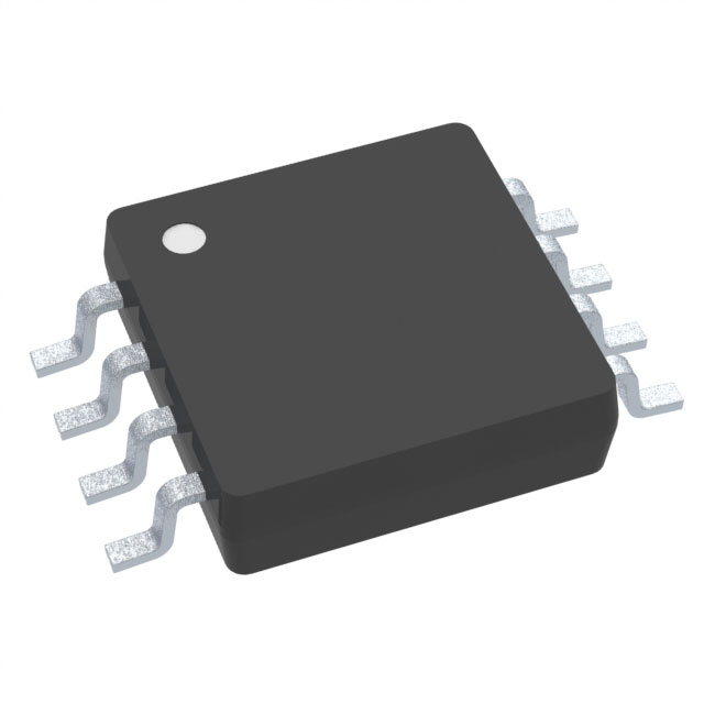
TLV9002IDGKT

Why Choose Us?
Professional Platform
B2B & B2C purchasingDelivery at full speed
1-2 days deliveryWide variety
Original manufacturers365 days guarantee
Responsible quality
.png)


Tech Specifications
TLV9002IDGKT Description
The Texas Instruments TLV9002IDGKT is a high-performance, monolithic, fully integrated linear voltage regulator in a thermally enhanced 8-pin package. It is designed to provide a stable and reliable output voltage for a wide range of input voltages and load currents.
Description:
The TLV9002IDGKT is a low-dropout (LDO) voltage regulator that offers excellent line and load regulation. It has a very low dropout voltage, which allows it to operate efficiently even with a small input-to-output voltage difference. The device also features a low quiescent current, which makes it ideal for battery-powered applications.
Features:
- Low dropout voltage: The TLV9002IDGKT has a low dropout voltage of typically 300mV at 1A output current, which allows it to operate efficiently with a small input-to-output voltage difference.
- High output current: The device can provide a continuous output current of up to 1A, making it suitable for a wide range of applications.
- Low quiescent current: The TLV9002IDGKT has a low quiescent current of typically 70µA, which helps to extend the battery life in portable applications.
- Wide input voltage range: The device can operate with input voltages from 2.5V to 5.5V, making it suitable for a variety of power supply scenarios.
- Thermally enhanced package: The TLV9002IDGKT is available in an 8-pin thermally enhanced package, which provides improved thermal performance and allows for better heat dissipation.
Applications:
The TLV9002IDGKT is suitable for a wide range of applications that require a stable and reliable output voltage. Some of the key applications include:
- Portable devices: The low quiescent current and low dropout voltage make the TLV9002IDGKT ideal for use in battery-powered devices such as smartphones, tablets, and wearable electronics.
- Power supplies: The device can be used in power supply applications where a stable and regulated output voltage is required, such as in industrial equipment, medical devices, and telecommunications equipment.
- Automotive: The TLV9002IDGKT can be used in automotive applications where a stable voltage supply is required for various electronic systems, such as infotainment systems, lighting, and engine control modules.
- IoT devices: The low power consumption and high output current capabilities make the TLV9002IDGKT suitable for use in Internet of Things (IoT) devices, such as sensors, smart home appliances, and security systems.
In summary, the Texas Instruments TLV9002IDGKT is a high-performance, low-dropout voltage regulator that offers excellent line and load regulation, low quiescent current, and a wide input voltage range. Its thermally enhanced package provides improved thermal performance, making it suitable for a wide range of applications, including portable devices, power supplies, automotive systems, and IoT devices.
FAQ
Not available to buy online? Want the lower wholesale price? Please Send RFQ to get best price, we will respond immediately


.png?x-oss-process=image/format,webp/resize,h_32)


