
 German
 Japanese
 Portuguese
 Korea
Korea
 Mexico
 Dutch
Dutch


Texas Instruments
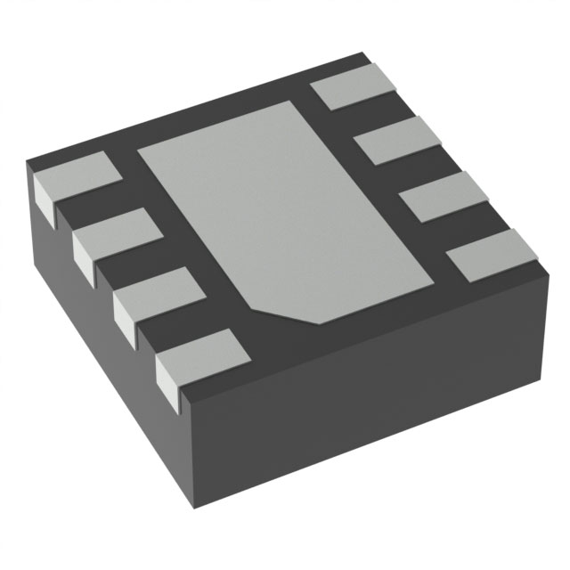
TLV9002IDSGT

Why Choose Us?
Professional Platform
B2B & B2C purchasingDelivery at full speed
1-2 days deliveryWide variety
Original manufacturers365 days guarantee
Responsible quality
.png)


Tech Specifications
TLV9002IDSGT Description
The TLV9002IDSGT is a low-power, single-supply, monolithic, 8-bit video decoder designed for use in battery-powered applications such as portable video equipment, digital still cameras, and security systems. It is manufactured by Texas Instruments.
Description:
The TLV9002IDSGT is a high-performance video decoder that can accept both composite and S-video inputs. It features a single-supply operation, which simplifies the power supply design and reduces power consumption. The device also includes an on-chip video gain control, which allows for easy adjustment of the video signal level.
Features:
- Single-supply operation
- Accepts both composite and S-video inputs
- On-chip video gain control
- Low-power consumption
- Small package size (DSGT package)
Applications:
The TLV9002IDSGT is suitable for a wide range of applications that require a low-power, single-supply video decoder. Some of the potential applications include:
- Portable video equipment
- Digital still cameras
- Security systems
- Video baby monitors
- Video conferencing systems
- Medical imaging equipment
- Industrial vision systems
In summary, the TLV9002IDSGT is a versatile and low-power video decoder that is well-suited for a variety of battery-powered applications. Its small package size and single-supply operation make it an ideal choice for portable and space-constrained systems.
FAQ
Not available to buy online? Want the lower wholesale price? Please Send RFQ to get best price, we will respond immediately


.png?x-oss-process=image/format,webp/resize,h_32)


