Texas Instruments_TLV9041IDBVR

Texas Instruments
TLV9041IDBVR  
OP Amps, Buffer Amps ICs

Texas Instruments
TLV9041IDBVR
687-TLV9041IDBVR
Ersa
Texas Instruments-TLV9041IDBVR-datasheets-4150217.pdf
IC OPAMP GP 1 CIRCUIT SOT23-5
In Stock : 48972

Not available to buy online? Want the lower wholesale price? Please Send RFQ to get best price, we will respond immediately

QUICK RFQ
ADD TO RFQ LIST
ersa FreeSample ersa flow
  • Quantity
  • Unit Price
  • Ext. Price
    • 1+
    • $0.23350
    • $0.23
    • 10+
    • $0.22687
    • $2.27
    • 30+
    • $0.22190
    • $6.66
    ADD TO CART
    QUICK ORDER
    $0.23350    $0.23
    ISO9001
    Quality Policy
    ISO45001
    ISO14001

    TLV9041IDBVR Description

    TLV9041IDBVR Description

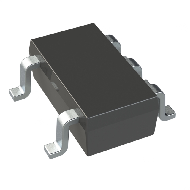
    The TLV9041IDBVR is a high-performance operational amplifier (op-amp) from Texas Instruments, designed for a wide range of applications requiring precision and reliability. This single-circuit op-amp is housed in a compact SOT23-5 package, making it ideal for space-constrained designs. With a supply voltage range of 1.2V to 5.5V, the TLV9041IDBVR offers flexibility in various power supply configurations.

    TLV9041IDBVR Features

    • Voltage - Supply Span (Min/Max): 1.2V to 5.5V, providing versatility in power supply options.
    • Gain Bandwidth Product: 350 kHz, ensuring high-speed amplification capabilities.
    • Slew Rate: 0.2V/µs, enabling rapid response to input signal changes.
    • Current - Supply: 10µA, contributing to low-power consumption in battery-operated devices.
    • Current - Input Bias: 1 pA, minimizing input offset error and improving overall accuracy.
    • Voltage - Input Offset: 600 µV, offering precise input signal processing.
    • Mounting Type: Surface Mount, suitable for PCB integration in compact electronic devices.
    • Number of Circuits: 1, making it suitable for single-channel amplification applications.
    • Amplifier Type: General Purpose, versatile enough for a wide range of applications.
    • Current - Output / Channel: 40 mA, capable of driving various loads.
    • RoHS Status: ROHS3 Compliant, adhering to environmental regulations.
    • Moisture Sensitivity Level (MSL): 1 (Unlimited), indicating no special precautions are needed for handling and storage.

    TLV9041IDBVR Applications

    The TLV9041IDBVR's combination of low power consumption, high slew rate, and precision amplification make it an excellent choice for applications such as:

    • Sensor Signal Conditioning: Its low input bias current and low offset voltage are ideal for conditioning signals from precision sensors.
    • Portable Electronics: The low supply current is beneficial for extending battery life in portable devices.
    • Audio Amplification: The high slew rate and bandwidth make it suitable for audio signal processing in consumer electronics.
    • Industrial Control Systems: Its general-purpose nature and robust performance characteristics are well-suited for various control applications.

    Conclusion of TLV9041IDBVR

    The TLV9041IDBVR from Texas Instruments stands out for its versatility, precision, and reliability in op-amp applications. Its unique combination of technical specifications, such as a wide supply voltage range, low power consumption, and high slew rate, positions it as a preferred choice for a variety of electronic systems. Whether used in sensor signal conditioning, portable electronics, or industrial control systems, the TLV9041IDBVR delivers consistent performance and value.

    Tech Specifications

    Number of Channels per Chip
    Power Supply Type
    Rail-to-rail
    Product
    PPAP
    Gain Bandwidth Product
    Automotive
    Maximum Input Offset Current (uA)
    RoHS
    THD plus Noise
    REACH Status
    Input common mode headroom (to negative supply) (typ) (V)
    Operating temperature range (°C)
    Current - Supply
    Output swing headroom (to negative supply) (typ) (V)
    Standard Package Name
    Shut Down Support
    Mounting
    Minimum Single Supply Voltage (V)
    Iout (typ) (A)
    Manufacturer Type
    Package
    Minimum CMRR (dB)
    Total supply voltage (+5 V = 5, ±5 V = 10) (max) (V)
    GBW (typ) (MHz)
    en - Input Voltage Noise Density
    Output Type
    Vos - Input Offset Voltage
    Minimum CMRR Range (dB)
    Typical Gain Bandwidth Product (MHz)
    Package Height
    Maximum Operating Temperature
    Ib - Input Bias Current
    RoHS Status
    Number of channels
    Iq per channel (typ) (mA)
    Minimum Operating Temperature
    Voltage - Input Offset
    Type
    Vos (offset voltage at 25°C) (max) (mV)
    Output Current per Channel
    Part Status
    Lead finish / Ball material
    Number of Circuits
    Package Width
    GBP - Gain Bandwidth Product
    Voltage - Supply Span (Max)
    Maximum Input Offset Voltage (mV)
    Product Status
    Current - Input Bias
    Rail to Rail
    Supplier Package
    Package / Case
    Number of Channels
    Typical Voltage Gain (dB)
    EU RoHS
    Carrier
    Amplifier Type
    Maximum Dual Supply Voltage (V)
    Input common mode headroom (to positive supply) (typ) (V)
    Moisture Sensitivity Level (MSL)
    Typical Input Noise Voltage Density (nV/rtHz)
    Operating Temperature
    Architecture
    Typical Slew Rate (V/us)
    Output swing headroom (to positive supply) (typ) (V)
    ECCN
    MSL rating / Peak reflow
    Mounting Type
    Pin Count
    In - Input Noise Current Density
    Ios - Input Offset Current
    Minimum PSRR (dB)
    Shutdown
    Voltage - Supply Span (Min)
    HTSUS
    Pins
    Current - Output / Channel
    USHTS
    PCB changed
    HTS
    Rating
    ECCN (US)
    Total supply voltage (+5 V = 5, ±5 V = 10) (min) (V)
    Supplier Device Package
    Supply Voltage - Min
    Minimum Operating Temperature (°C)
    Maximum Operating Temperature (°C)
    Operating Supply Current
    SR - Slew Rate
    Mfr
    Features
    CMRR (typ) (dB)
    Supply Voltage - Max
    Offset drift (typ) (µV/°C)
    Mounting Style
    Input Type
    Maximum Input Bias Current (uA)
    Typical Noninverting Input Current Noise Density (pA/rtHz)
    Slew Rate
    Package Length
    Minimum Dual Supply Voltage (V)
    Vn at 1 kHz (typ) (nV√Hz)
    CMRR - Common Mode Rejection Ratio
    REACH
    Series
    Maximum Single Supply Voltage (V)
    Slew rate (typ) (V/µs)
    Typical Settling Time (ns)
    Input bias current (max) (pA)

    TLV9041IDBVR Documents

    Download datasheets and manufacturer documentation for TLV9041IDBVR

    Ersa Product Change Notification (PDF)       Product Change Notification 2024-06-24 (PDF)      

    Shopping Guide

    Payment Methods
    Payment Methods include Prepayment TT (bank transfer), Western Union, and PayPal. Customers are responsible for shipping costs, bank charges, customs duties and taxes.
    Shipping Rate
    Shipments are made once a day around 5pm, excluding Sundays. Once shipped, the estimated delivery time is usually 5-7 business days, depending on the courier you choose.
    Delivery Methods
    Provide DHL, FedEx, UPS, EMS, SF Express and Registered Airmail International Delivery Service