
 German
 Japanese
 Portuguese
 Korea
Korea
 Mexico
 Dutch
Dutch


Texas Instruments
TLV9052IDSGR

Why Choose Us?
Professional Platform
B2B & B2C purchasingDelivery at full speed
1-2 days deliveryWide variety
Original manufacturers365 days guarantee
Responsible quality
.png)


Tech Specifications
TLV9052IDSGR Description
TLV9052IDSGR Description
The TLV9052IDSGR is a high-performance CMOS operational amplifier from Texas Instruments, designed for a wide range of applications requiring precision and low power consumption. This dual-channel amplifier features a supply voltage range of 1.8 V to 5.5 V, making it suitable for both low-power and standard voltage systems. With a gain bandwidth product of 5 MHz and a slew rate of 15 V/µs, the TLV9052IDSGR offers excellent performance in high-frequency applications. The device also boasts a low input bias current of 2 pA and an input offset voltage of 330 µV, ensuring high accuracy and stability in signal processing.
TLV9052IDSGR Features
- Low Power Consumption: The TLV9052IDSGR operates with a supply current of just 330 µA, making it ideal for battery-powered and energy-sensitive applications.
- Wide Supply Voltage Range: With an operational supply voltage range from 1.8 V to 5.5 V, this amplifier can be used in a variety of systems, from low-voltage portable devices to standard 5 V systems.
- High Gain Bandwidth Product: The 5 MHz gain bandwidth product ensures high-frequency performance, making it suitable for applications requiring fast signal processing.
- High Slew Rate: The 15 V/µs slew rate allows for rapid response to input signal changes, minimizing distortion in high-speed applications.
- Low Input Bias Current: The 2 pA input bias current ensures minimal loading on the input signal source, preserving signal integrity.
- Low Input Offset Voltage: The 330 µV input offset voltage contributes to high accuracy and precision in signal amplification.
- Dual Channel Design: The TLV9052IDSGR features two independent amplifier circuits, allowing for compact and efficient designs in multi-channel applications.
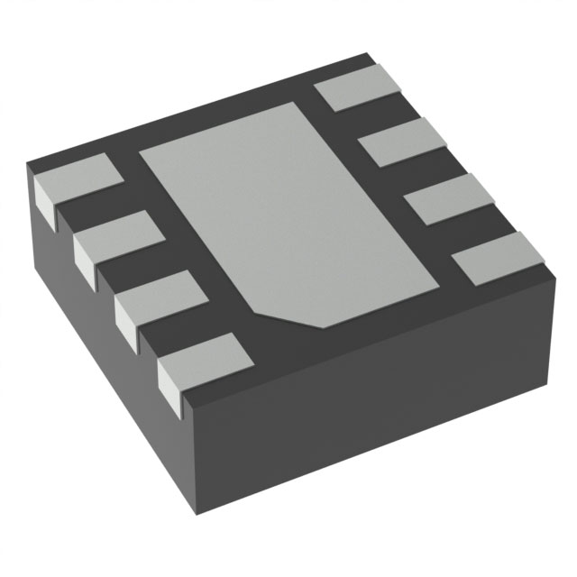
- Surface Mount Packaging: The 8WSON package is designed for surface mount technology, enabling high-density PCB layouts and automated assembly processes.
TLV9052IDSGR Applications
The TLV9052IDSGR is well-suited for a variety of applications across different industries, including:
- Consumer Electronics: Ideal for portable devices such as smartphones, tablets, and wearables where low power consumption and high performance are critical.
- Industrial Automation: Used in sensor interfaces, signal conditioning, and control systems where precision and reliability are paramount.
- Medical Devices: Suitable for medical equipment requiring high accuracy and low power, such as portable diagnostic devices and wearable health monitors.
- Automotive Electronics: Applicable in automotive systems for signal processing and control, benefiting from the wide supply voltage range and robust performance.
- Communication Systems: Effective in communication infrastructure for signal amplification and conditioning, ensuring high-speed and reliable performance.
Conclusion of TLV9052IDSGR
The TLV9052IDSGR from Texas Instruments stands out as a versatile and high-performance CMOS operational amplifier. Its combination of low power consumption, wide supply voltage range, and high-frequency performance makes it an excellent choice for a variety of applications. The dual-channel design and surface mount packaging further enhance its suitability for modern, compact electronic systems. Whether in consumer electronics, industrial automation, or medical devices, the TLV9052IDSGR offers a reliable and efficient solution for precision signal processing.
FAQ
Not available to buy online? Want the lower wholesale price? Please Send RFQ to get best price, we will respond immediately


.png?x-oss-process=image/format,webp/resize,h_32)


