
Texas Instruments
TLV9052IPWR
OP Amps, Buffer Amps ICs


- 1+
- $0.39413
- $0.39
- 10+
- $0.32126
- $3.21
- 30+
- $0.28980
- $8.69
- 100+
- $0.25006
- $25.01
- 500+
- $0.23350
- $116.75
- 1000+
- $0.22190
- $221.9

.png?x-oss-process=image/format,webp/resize,p_30)


TLV9052IPWR Description
TLV9052IPWR Description
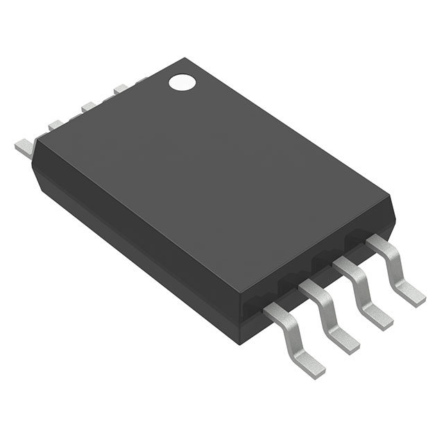
The TLV9052IPWR is a high-performance, dual-channel operational amplifier (op-amp) from Texas Instruments. It is designed using CMOS technology and is available in an 8-pin TSSOP package. This op-amp offers a wide supply voltage range from 1.8V to 5.5V, making it suitable for a variety of low-voltage applications. With a gain bandwidth product of 5 MHz and a slew rate of 15V/µs, the TLV9052IPWR delivers excellent high-frequency performance.
TLV9052IPWR Features
- Wide Supply Voltage Range: 1.8V to 5.5V, allowing for compatibility with various power sources.
- High Gain Bandwidth Product: 5 MHz, enabling high-speed signal processing.
- Fast Slew Rate: 15V/µs, ensuring quick response to input changes.
- Low Input Bias Current: 2 pA, minimizing input offset errors.
- Low Input Offset Voltage: 330 µV, improving accuracy in precision applications.
- Low Supply Current: 330 µA, suitable for power-sensitive designs.
- High Output Current: 50 mA per channel, capable of driving demanding loads.
- REACH Unaffected Status: Compliant with European chemical regulations.
- RoHS3 Compliance: Adheres to environmental standards.
- Moisture Sensitivity Level 2: Suitable for standard storage conditions.
- Surface Mount Packaging: Facilitates integration into modern electronic designs.
TLV9052IPWR Applications
The TLV9052IPWR's combination of high performance and low power consumption makes it ideal for a variety of applications:
- Audio Amplification: Its low distortion and high slew rate make it suitable for audio signal processing.
- Sensor Conditioning: The low input bias current and offset voltage are beneficial for accurate sensor signal amplification.
- Data Acquisition Systems: The wide supply range and high gain bandwidth product support various data acquisition tasks.
- Portable Electronics: The low power consumption is advantageous for battery-powered devices.
- Industrial Control Systems: Reliable operation in a wide range of supply voltages is crucial for industrial applications.
Conclusion of TLV9052IPWR
The TLV9052IPWR from Texas Instruments stands out for its versatility and performance in low-voltage, high-speed applications. Its unique combination of a wide supply voltage range, low power consumption, and high slew rate positions it as a preferred choice for designers looking to optimize both performance and power efficiency. With its compliance to environmental standards and robust technical specifications, the TLV9052IPWR is a reliable component for a broad spectrum of electronic systems.
Tech Specifications
TLV9052IPWR Documents
Download datasheets and manufacturer documentation for TLV9052IPWR
 Product Change Notification 2024-03-04 (PDF) Product Change Notification (PDF)
  TLV9052IPWR Symbol & Footprint by SnapMagic
  Second-sourcing options for small-package amplifiers Low Voltage High Slew Rate Op-amps for Motor Drive Circuits Sine wave generator circuit
  TLV9052 TINA-TI Reference Design (Rev. B)
  TLV9052 PSPICE Model (Rev. B)
 Shopping Guide


.png?x-oss-process=image/format,webp/resize,h_32)


