Texas Instruments_TLV9061SIDBVR

Texas Instruments
TLV9061SIDBVR  
OP Amps, Buffer Amps ICs

Texas Instruments
TLV9061SIDBVR
687-TLV9061SIDBVR
Ersa
Texas Instruments-TLV9061SIDBVR-datasheets-5548019.pdf
IC CMOS 1 CIRCUIT SOT23-6
In Stock : 4547

Not available to buy online? Want the lower wholesale price? Please Send RFQ to get best price, we will respond immediately

QUICK RFQ
ADD TO RFQ LIST
ersa FreeSample ersa flow
  • Quantity
  • Unit Price
  • Ext. Price
    • 1+
    • $0.47693
    • $0.48
    • 10+
    • $0.37922
    • $3.79
    • 30+
    • $0.33617
    • $10.09
    • 100+
    • $0.28483
    • $28.48
    • 500+
    • $0.26165
    • $130.82
    ADD TO CART
    QUICK ORDER
    $0.47693    $0.48
    ISO9001
    Quality Policy
    ISO45001
    ISO14001

    TLV9061SIDBVR Description

    The TLV9061SIDBVR is a low-power, high-precision monolithic CMOS operational amplifier (op-amp) from Texas Instruments. It is designed for use in a wide range of applications that require high accuracy and low power consumption, such as battery-powered devices, portable equipment, and precision measurement systems.

    Description:

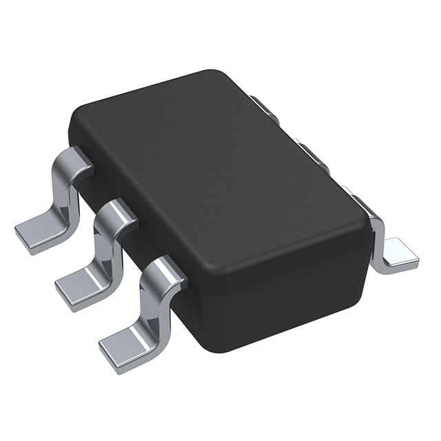
    The TLV9061SIDBVR is an 8-pin surface-mount package that features a single op-amp with a high input impedance, low input offset voltage, and low input bias current. It is available in a small-outline integrated circuit (SOIC) package, making it suitable for space-constrained applications.

    Features:

    1. Low power consumption: The TLV9061SIDBVR consumes only 45 µA per (amplifier) at a 5 V supply voltage, making it ideal for battery-powered applications.
    2. High precision: The op-amp offers an input offset voltage of typically 1 µV max and an input bias current of typically 1 pA, providing excellent accuracy for precision measurements.
    3. Wide supply voltage range: The TLV9061SIDBVR operates over a supply voltage range of 2.7 V to 10 V, allowing it to be used in various applications with different power supply requirements.
    4. Low drift: The device has a low temperature drift of 0.2 µV/°C for the input offset voltage and 0.5 pA/°C for the input bias current, ensuring stable performance over a wide temperature range.
    5. Rail-to-rail input and output: The TLV9061SIDBVR features rail-to-rail input and output, allowing it to operate with input signals that are close to the supply voltage rails.

    Applications:

    1. Battery-powered devices: Due to its low power consumption, the TLV9061SIDBVR is well-suited for use in battery-powered devices such as portable data loggers, medical equipment, and wireless sensors.
    2. Precision measurement systems: The high accuracy and low drift of the TLV9061SIDBVR make it an excellent choice for precision measurement systems, including temperature, pressure, and humidity sensors.
    3. Strain gauge amplifiers: The low input offset voltage and low drift of the TLV9061SIDBVR make it suitable for use in strain gauge amplifiers for applications such as force and torque measurement.
    4. pH meters and chemical sensors: The TLV9061SIDBVR can be used in pH meters and other chemical sensors that require high accuracy and low drift.
    5. Audio equipment: The low noise and high accuracy of the TLV9061SIDBVR make it suitable for use in audio preamplifiers and other audio processing applications.

    In summary, the TLV9061SIDBVR is a low-power, high-precision op-amp from Texas Instruments that is suitable for a wide range of applications requiring accurate measurements and low power consumption. Its features, such as low input offset voltage, low input bias current, and low drift, make it an excellent choice for battery-powered devices, precision measurement systems, and other applications where accuracy and low power consumption are critical.

    Tech Specifications

    Number of Channels per Chip
    Unit Weight
    Power Supply Type
    Rail-to-rail
    Product
    PPAP
    Gain Bandwidth Product
    Automotive
    RoHS
    REACH Status
    Input common mode headroom (to negative supply) (typ) (V)
    Operating temperature range (°C)
    PSRR - Power Supply Rejection Ratio
    Supplier Temperature Grade
    Current - Supply
    Output swing headroom (to negative supply) (typ) (V)
    Standard Package Name
    Shut Down Support
    Mounting
    Minimum Single Supply Voltage (V)
    Iout (typ) (A)
    Manufacturer Type
    Package
    Minimum CMRR (dB)
    Total supply voltage (+5 V = 5, ±5 V = 10) (max) (V)
    GBW (typ) (MHz)
    en - Input Voltage Noise Density
    Output Type
    Vos - Input Offset Voltage
    Minimum CMRR Range (dB)
    Process Technology
    Typical Gain Bandwidth Product (MHz)
    Package Height
    Maximum Operating Temperature
    Ib - Input Bias Current
    RoHS Status
    Number of channels
    Iq per channel (typ) (mA)
    Minimum Operating Temperature
    Voltage - Input Offset
    Type
    Vos (offset voltage at 25°C) (max) (mV)
    Output Current per Channel
    Part Status
    Lead finish / Ball material
    Number of Circuits
    Package Width
    GBP - Gain Bandwidth Product
    Voltage - Supply Span (Max)
    Maximum Input Offset Voltage (mV)
    Product Status
    Rail to Rail
    Supplier Package
    Package / Case
    Number of Channels
    Typical Voltage Gain (dB)
    Typical Input Bias Current (uA)
    EU RoHS
    Carrier
    Amplifier Type
    Input common mode headroom (to positive supply) (typ) (V)
    Moisture Sensitivity Level (MSL)
    Typical Input Noise Voltage Density (nV/rtHz)
    Operating Temperature
    Architecture
    Typical Slew Rate (V/us)
    Output swing headroom (to positive supply) (typ) (V)
    ECCN
    MSL rating / Peak reflow
    Mounting Type
    Pin Count
    In - Input Noise Current Density
    Ios - Input Offset Current
    Minimum PSRR (dB)
    Shutdown
    Voltage - Supply Span (Min)
    Lead Shape
    SVHC
    HTSUS
    Pins
    Current - Output / Channel
    USHTS
    PCB changed
    HTS
    Rating
    ECCN (US)
    Total supply voltage (+5 V = 5, ±5 V = 10) (min) (V)
    Supplier Device Package
    Supply Voltage - Min
    Minimum Operating Temperature (°C)
    Maximum Operating Temperature (°C)
    Operating Supply Current
    SR - Slew Rate
    Mfr
    Features
    CMRR (typ) (dB)
    Supply Voltage - Max
    Offset drift (typ) (µV/°C)
    Mounting Style
    Input Type
    Typical Noninverting Input Current Noise Density (pA/rtHz)
    Slew Rate
    Package Length
    Vn at 1 kHz (typ) (nV√Hz)
    CMRR - Common Mode Rejection Ratio
    REACH
    Series
    Maximum Single Supply Voltage (V)
    Slew rate (typ) (V/µs)
    Typical Settling Time (ns)
    Base Product Number

    TLV9061SIDBVR Documents

    Download datasheets and manufacturer documentation for TLV9061SIDBVR

    Ersa Assembly Material 13/Jul/2023      
    Ersa TLV906x Datasheet      
    Ersa SOT Symbolization update 09/Sep/2019      
    Ersa TLV906x Datasheet      
    Ersa TLV9061/TLV9062/TLV9064 08/Oct/2019      

    Shopping Guide

    Payment Methods
    Payment Methods include Prepayment TT (bank transfer), Western Union, and PayPal. Customers are responsible for shipping costs, bank charges, customs duties and taxes.
    Shipping Rate
    Shipments are made once a day around 5pm, excluding Sundays. Once shipped, the estimated delivery time is usually 5-7 business days, depending on the courier you choose.
    Delivery Methods
    Provide DHL, FedEx, UPS, EMS, SF Express and Registered Airmail International Delivery Service