
 German
 Japanese
 Portuguese
 Korea
Korea
 Mexico
 Dutch
Dutch


Texas Instruments
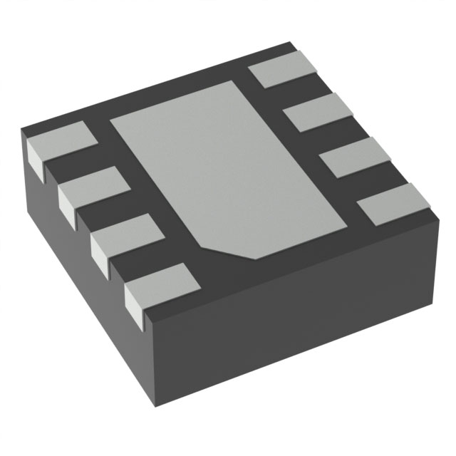
TLV9062IDSGR

Why Choose Us?
Professional Platform
B2B & B2C purchasingDelivery at full speed
1-2 days deliveryWide variety
Original manufacturers365 days guarantee
Responsible quality
.png)


Tech Specifications
TLV9062IDSGR Description
The TLV9062IDSGR is a high-precision, low-power, monolithic CMOS operational amplifier (op-amp) from Texas Instruments. It is designed to provide excellent DC and AC performance, making it suitable for a wide range of applications.
Description:
The TLV9062 is a low-voltage, precision operational amplifier with a wide supply voltage range of 2.7V to 5.5V. It features a low input offset voltage of 1µV max and a low input bias current of 1pA max. The device also has a high open-loop gain of 120dB and a low output noise of 7nV/√Hz.
Features:
- Low input offset voltage: 1µV max
- Low input bias current: 1pA max
- Wide supply voltage range: 2.7V to 5.5V
- High open-loop gain: 120dB
- Low output noise: 7nV/√Hz
- Precision performance: suitable for use in a variety of precision applications
- Low power consumption: suitable for battery-powered applications
- Available in a small SOT-23 package
Applications:
The TLV9062 is suitable for a wide range of applications that require precision amplification, including:
- Strain gauge amplifiers
- Medical instrumentation
- pH meter amplifiers
- Pressure sensor amplifiers
- Battery-powered applications
- Data acquisition systems
- Industrial control systems
- Audio equipment
- Temperature measurement systems
In summary, the TLV9062IDSGR is a high-precision, low-power op-amp from Texas Instruments that is suitable for a wide range of applications that require precision amplification. Its low input offset voltage, low input bias current, and low output noise make it an excellent choice for use in a variety of precision applications.
FAQ
| Quantity | Unit Price | Ext. Price |
|---|---|---|
| 10+ | $0.56228 | $5.62 |
| 30+ | $0.49715 | $14.91 |
| 100+ | $0.43200 | $43.20 |
| 500+ | $0.39428 | $197.14 |
| 1000+ | $0.37372 | $373.72 |
Not available to buy online? Want the lower wholesale price? Please Send RFQ to get best price, we will respond immediately


.png?x-oss-process=image/format,webp/resize,h_32)


