
Texas Instruments
TLV9062QPWRQ1
OP Amps, Buffer Amps ICs


.png?x-oss-process=image/format,webp/resize,p_30)


TLV9062QPWRQ1 Description
TLV9062QPWRQ1 Description
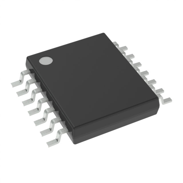
The TLV9062QPWRQ1 is an automotive-grade, dual-channel operational amplifier designed for high performance and reliability in demanding applications. Manufactured by Texas Instruments, this IC features a wide supply voltage range from 1.8 V to 5.5 V, making it suitable for various power supply configurations. With a gain bandwidth product of 10 MHz and a slew rate of 6.5 V/µs, the TLV9062QPWRQ1 ensures fast and accurate signal processing. Its low input bias current of 5 pA and input offset voltage of 300 µV contribute to high precision and stability in signal amplification.
TLV9062QPWRQ1 Features
- Wide Supply Voltage Range: Operates from 1.8 V to 5.5 V, providing flexibility in power supply design.
- High Gain Bandwidth Product: 10 MHz ensures high-frequency performance, making it suitable for applications requiring fast signal processing.
- Low Input Bias Current: 5 pA minimizes the impact on sensitive input signals, ensuring high precision.
- Low Input Offset Voltage: 300 µV ensures accurate amplification and minimal error in signal processing.
- High Slew Rate: 6.5 V/µs allows for rapid response to input signal changes, maintaining signal integrity.
- Dual Channel Design: Two independent amplifiers in a single package, ideal for space-constrained designs.
- Automotive Grade: Designed to meet the stringent requirements of automotive applications, ensuring reliability and performance in harsh environments.
- Compliance: REACH Unaffected and RoHS3 Compliant, ensuring environmental and safety standards are met.
- Moisture Sensitivity Level: MSL 2 (1 Year), suitable for surface mount assembly processes.
- Packaging: Tape & Reel (TR) for efficient manufacturing and handling.
TLV9062QPWRQ1 Applications
The TLV9062QPWRQ1 is ideal for a variety of automotive applications where high performance and reliability are critical. Some specific use cases include:
- Automotive Sensing: Ideal for amplifying signals from sensors in automotive systems, such as temperature, pressure, and position sensors.
- Infotainment Systems: Provides high-quality signal processing for audio and video applications, ensuring clear and accurate output.
- Safety Systems: Suitable for applications like advanced driver-assistance systems (ADAS), where precise signal processing is essential for safety.
- Power Management: Effective in managing and conditioning power signals in automotive electronic control units (ECUs).
Conclusion of TLV9062QPWRQ1
The TLV9062QPWRQ1 from Texas Instruments is a robust and versatile dual-channel operational amplifier designed specifically for automotive applications. Its wide supply voltage range, high gain bandwidth product, and low input bias current make it an excellent choice for applications requiring high precision and fast signal processing. The automotive-grade design ensures reliability and performance in harsh environments, while compliance with REACH and RoHS3 standards ensures environmental and safety requirements are met. With its dual-channel configuration and efficient packaging, the TLV9062QPWRQ1 is an ideal solution for space-constrained designs, making it a standout choice in the market.
Tech Specifications
TLV9062QPWRQ1 Documents
Download datasheets and manufacturer documentation for TLV9062QPWRQ1
 TLV906xS-Q1
  MSL Improvement for Select Devices 28/Aug/2023
  Mult PN PART MARKING 08/Dec/2023
 Shopping Guide


.png?x-oss-process=image/format,webp/resize,h_32)


