
 German
 Japanese
 Portuguese
 Korea
Korea
 Mexico
 Dutch
Dutch


Texas Instruments
TLV9064IPWT

Why Choose Us?
Professional Platform
B2B & B2C purchasingDelivery at full speed
1-2 days deliveryWide variety
Original manufacturers365 days guarantee
Responsible quality
.png)


Tech Specifications
TLV9064IPWT Description
TLV9064IPWT Description
The TLV9064IPWT is a high-performance CMOS operational amplifier from Texas Instruments, designed for a wide range of applications requiring precision and low power consumption. This quad-channel amplifier operates within a supply voltage range of 1.8 V to 5.5 V, making it suitable for both low-voltage and standard voltage systems. The TLV9064IPWT features a gain bandwidth product of 10 MHz, ensuring high-frequency performance and stability. With a slew rate of 6.5 V/µs, it can handle fast signal transitions without distortion.
TLV9064IPWT Features
- Low Power Consumption: The TLV9064IPWT consumes only 538 µA across four channels, making it ideal for battery-powered and energy-efficient designs.
- High Input Impedance: With an input bias current of just 0.5 pA, this amplifier minimizes loading effects on sensitive input sources.
- Low Input Offset Voltage: The 300 µV input offset voltage ensures high accuracy and precision in signal processing.
- Wide Supply Voltage Range: Operating from 1.8 V to 5.5 V, the TLV9064IPWT is versatile and can be used in a variety of power supply environments.
- High Output Current: Each channel can deliver up to 50 mA, providing robust performance for driving various loads.
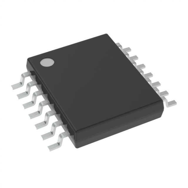
- Surface Mount Technology: The 14-TSSOP package is designed for surface mount applications, ensuring ease of integration into modern PCB designs.
- Compliance and Reliability: The TLV9064IPWT is REACH unaffected and RoHS3 compliant, ensuring environmental and regulatory compliance. It also has a moisture sensitivity level (MSL) of 2, suitable for long-term storage.
TLV9064IPWT Applications
The TLV9064IPWT is well-suited for a variety of applications where precision, low power, and high performance are critical. Key applications include:
- Signal Conditioning: Ideal for amplifying and conditioning low-level signals in sensor interfaces and analog front-ends.
- Battery-Powered Devices: Its low power consumption makes it suitable for portable electronics and IoT devices.
- Medical Equipment: The high precision and low noise characteristics are beneficial for medical instrumentation and diagnostic equipment.
- Industrial Automation: The robustness and wide operating voltage range make it suitable for industrial control systems and automation equipment.
- Consumer Electronics: Suitable for audio processing, signal amplification, and other consumer electronics applications requiring high performance and low power.
Conclusion of TLV9064IPWT
The TLV9064IPWT from Texas Instruments is a versatile and high-performance CMOS operational amplifier that stands out in its class. Its low power consumption, high input impedance, and wide supply voltage range make it an excellent choice for a variety of applications. The TLV9064IPWT offers precision and reliability, making it an ideal component for engineers looking to optimize their designs for performance and efficiency. Whether in medical, industrial, or consumer electronics, the TLV9064IPWT delivers the performance needed to meet the demands of modern electronic systems.
FAQ
Not available to buy online? Want the lower wholesale price? Please Send RFQ to get best price, we will respond immediately


.png?x-oss-process=image/format,webp/resize,h_32)


