
 German
 Japanese
 Portuguese
 Korea
Korea
 Mexico
 Dutch
Dutch


Texas Instruments
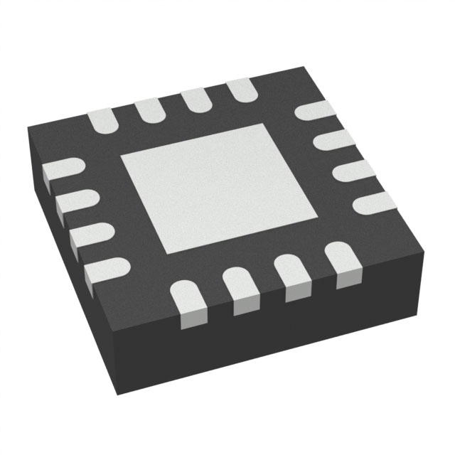
TLV9064IRTER

Why Choose Us?
Professional Platform
B2B & B2C purchasingDelivery at full speed
1-2 days deliveryWide variety
Original manufacturers365 days guarantee
Responsible quality
.png)


Tech Specifications
TLV9064IRTER Description
The TLV9064IRTER is a high-precision, low-power, 16-bit successive approximation register (SAR) analog-to-digital converter (ADC) from Texas Instruments. It is designed for use in a wide range of applications, including industrial, medical, and consumer electronics.
Description:
The TLV9064IRTER is a 16-bit SAR ADC that offers high resolution and accuracy. It has a wide input voltage range of 0V to 5.5V and supports both unipolar and bipolar inputs. The device features a low power consumption of 13.5µA in normal mode and 0.5µA in power-down mode, making it suitable for battery-powered applications.
Features:
- 16-bit resolution with no missing codes
- Wide input voltage range of 0V to 5.5V (unipolar) or -2.75V to +2.75V (bipolar)
- Low power consumption: 13.5µA in normal mode and 0.5µA in power-down mode
- Programmable conversion rate
- Internal oscillator for clock generation
- I2C and SPI compatible digital interfaces
- Small package size (6mm x 6mm TSSOP)
Applications:
- Industrial control systems
- Medical equipment
- Battery-powered devices
- Precision measurement instruments
- Data acquisition systems
- Smart sensors
- Energy harvesting systems
In summary, the TLV9064IRTER is a high-precision, low-power ADC that offers excellent resolution and accuracy for a wide range of applications. Its low power consumption, wide input voltage range, and small package size make it an ideal choice for battery-powered and space-constrained applications.
FAQ
Not available to buy online? Want the lower wholesale price? Please Send RFQ to get best price, we will respond immediately


.png?x-oss-process=image/format,webp/resize,h_32)


