

Texas Instruments
TLV9352IPWR
OP Amps, Buffer Amps ICs

Not available to buy online? Want the lower wholesale price? Please Send RFQ to get best price, we will respond immediately


.png?x-oss-process=image/format,webp/resize,p_30)


TLV9352IPWR Description
TLV9352IPWR Description
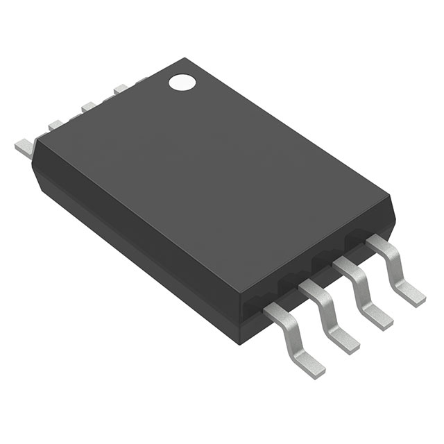
The TLV9352IPWR is a high-performance, general-purpose operational amplifier designed by Texas Instruments. This dual-channel op-amp is housed in an 8-pin TSSOP package, making it suitable for surface-mount applications. It is ideal for a wide range of analog signal processing tasks due to its robust performance characteristics and versatility.
TLV9352IPWR Features
- Wide Supply Voltage Range: The TLV9352IPWR operates over a wide supply voltage range from 4.5 V to 40 V, making it suitable for various power supply configurations.
- High Gain Bandwidth Product: With a gain bandwidth product of 3.5 MHz, this op-amp ensures high-frequency performance, making it ideal for applications requiring fast signal processing.
- Low Input Bias Current: The low input bias current of 10 pA minimizes the effect of input currents on the signal, ensuring high accuracy and stability in precision applications.
- High Slew Rate: The 20 V/µs slew rate allows for rapid changes in output voltage, making the TLV9352IPWR suitable for high-speed applications.
- Low Input Offset Voltage: The low input offset voltage of 350 µV ensures minimal error in the output signal, contributing to high accuracy in signal conditioning.
- Dual Channel Design: With two independent op-amp channels, the TLV9352IPWR can handle multiple signal paths, increasing the flexibility and efficiency of circuit design.
- Low Supply Current: The low supply current of 650 µA per channel ensures efficient power usage, making it suitable for battery-powered and low-power applications.
- High Output Current: Each channel can deliver up to 60 mA of output current, providing robust performance for driving various loads.
- Compliance and Reliability: The TLV9352IPWR is REACH unaffected and RoHS3 compliant, ensuring environmental and regulatory compliance. It also has a moisture sensitivity level (MSL) of 1, making it suitable for unlimited storage conditions.
TLV9352IPWR Applications
The TLV9352IPWR is well-suited for a variety of applications due to its versatile performance characteristics:
- Signal Conditioning: Ideal for amplifying, filtering, and conditioning analog signals in industrial and consumer electronics.
- Transducer Interfaces: Suitable for interfacing with various sensors and transducers, providing accurate signal processing and amplification.
- Power Management: Can be used in power supply circuits for voltage regulation and monitoring.
- Audio Applications: Its low noise and high slew rate make it suitable for audio signal processing, ensuring high-fidelity output.
- Medical Equipment: The low input bias current and high accuracy make it suitable for medical devices where precision is critical.
- Automotive Electronics: The wide supply voltage range and robust performance make it suitable for automotive applications where reliability and performance are paramount.
Conclusion of TLV9352IPWR
The TLV9352IPWR from Texas Instruments is a versatile and high-performance operational amplifier that offers a wide range of benefits for various applications. Its wide supply voltage range, high gain bandwidth product, low input bias current, and high slew rate make it an excellent choice for precision signal processing and high-speed applications. The dual-channel design and low supply current further enhance its flexibility and efficiency. With its compliance with environmental and regulatory standards, the TLV9352IPWR is a reliable and future-proof solution for modern electronics design.
Tech Specifications
TLV9352IPWR Documents
Download datasheets and manufacturer documentation for TLV9352IPWR
Product Change Notification (PDF) TLV9352IPWR Symbol & Footprint by SnapMagic TLV9352 TINA-TI Reference Design Model (Rev. A) TLV9352 TINA-TI Reference Design TLV9352 Pspice Model Related Parts


Shopping Guide


.png?x-oss-process=image/format,webp/resize,h_32)


©2025 ERSA Electronics Corporation.