
 German
 Japanese
 Portuguese
 Korea
Korea
 Mexico
 Dutch
Dutch


Texas Instruments
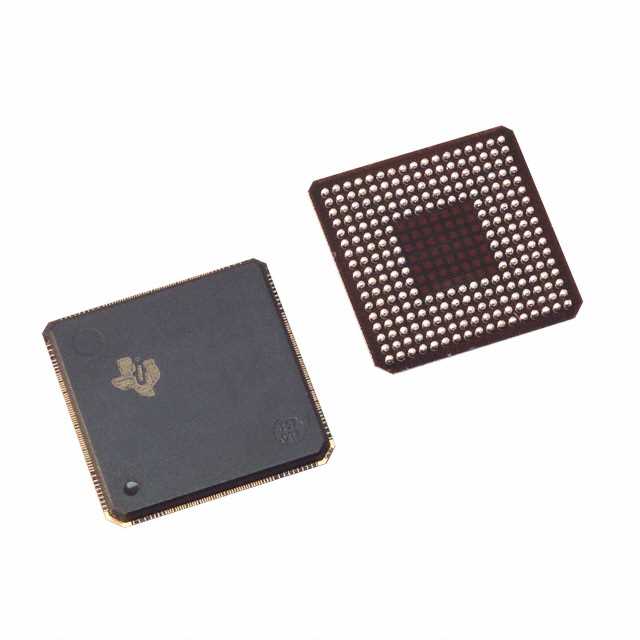
TMS320VC5510AZGW1

Why Choose Us?
Professional Platform
B2B & B2C purchasingDelivery at full speed
1-2 days deliveryWide variety
Original manufacturers365 days guarantee
Responsible quality
.png)


Tech Specifications
TMS320VC5510AZGW1 Description
TMS320VC5510AZGW1 Description
The TMS320VC5510AZGW1 is a high-performance fixed-point digital signal processor (DSP) from Texas Instruments' TMS320C55x series, designed for embedded signal processing applications. Packaged in a 240-BGA form factor, this DSP operates at a 160MHz clock rate with a 1.60V core voltage and 3.30V I/O voltage, balancing power efficiency and computational throughput. It integrates 344kB of on-chip RAM and 32kB of ROM, enabling rapid data access and firmware storage. The device supports Host Interface and McBSP (Multichannel Buffered Serial Port) for flexible communication with peripherals. Although marked as obsolete, it remains relevant in legacy systems due to its robust architecture and REACH/ROHS3 compliance.
TMS320VC5510AZGW1 Features
- High-Speed Processing: 160MHz clock rate ensures real-time signal processing for demanding algorithms.
- Memory Configuration: Combines 344kB RAM for data-intensive tasks and 32kB ROM for boot code.
- Low-Power Design: 1.60V core voltage minimizes energy consumption in portable applications.
- Versatile Interfaces: Host Interface and McBSP simplify integration with sensors, ADCs, and other DSPs.
- Industrial Robustness: Operates at 0°C to 85°C (TC) and is surface-mountable (MSL 3) for harsh environments.
- Legacy Compliance: ECCN 3A991A2 and HTSUS 8542.31.0001 certifications ensure global deployment compatibility.
TMS320VC5510AZGW1 Applications
- Telecommunications: Voice processing, echo cancellation, and modem algorithms.
- Audio Processing: Noise reduction, audio effects, and speech recognition in consumer electronics.
- Industrial Control: Motor control, predictive maintenance, and real-time sensor analytics.
- Medical Devices: Portable diagnostic equipment requiring low-power, high-speed DSP capabilities.
- Legacy System Upgrades: Ideal for retrofitting older designs due to its proven reliability and interface support.
Conclusion of TMS320VC5510AZGW1
The TMS320VC5510AZGW1 excels in fixed-point DSP applications where low power, high speed, and deterministic performance are critical. Its integrated memory and flexible interfaces make it suitable for telecommunications, audio, and industrial systems. While obsolete, its ROHS3 compliance and thermal resilience ensure longevity in existing deployments. Engineers seeking a cost-effective, proven DSP solution for legacy or niche applications will find this device a compelling choice.
FAQ
| Quantity | Unit Price | Ext. Price |
|---|---|---|
| 1+ | $28.40640 | $28.41 |
| 10+ | $23.01288 | $230.13 |
| 25+ | $21.66595 | $541.65 |
| 126+ | $19.99046 | $2518.80 |
Not available to buy online? Want the lower wholesale price? Please Send RFQ to get best price, we will respond immediately


.png?x-oss-process=image/format,webp/resize,h_32)


