
 German
 Japanese
 Portuguese
 Korea
Korea
 Mexico
 Dutch
Dutch



Texas Instruments
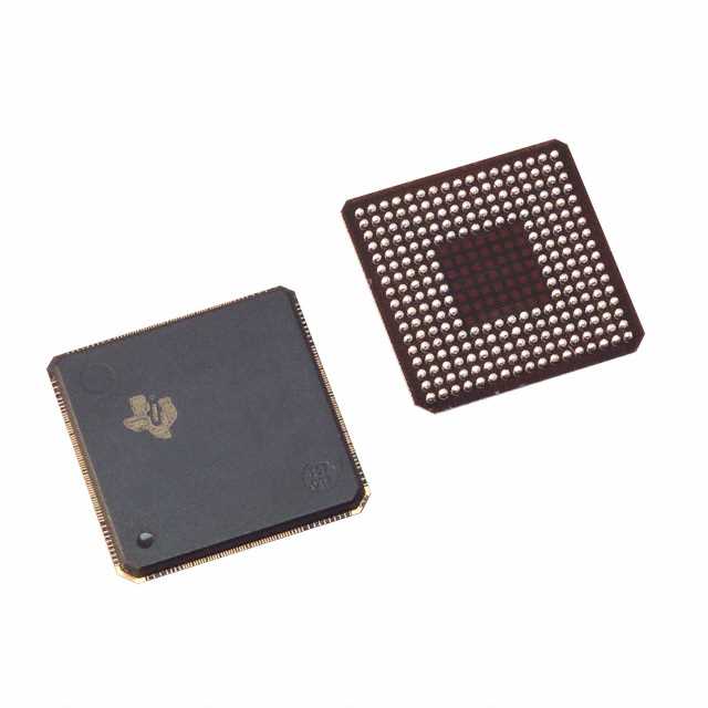
TMS320VC5510AZGWA1


Why Choose Us?
Professional Platform
B2B & B2C purchasingDelivery at full speed
1-2 days deliveryWide variety
Original manufacturers365 days guarantee
Responsible quality

.png)


Tech Specifications
TMS320VC5510AZGWA1 Description
TMS320VC5510AZGWA1 Description
The TMS320VC5510AZGWA1 is a high-performance fixed-point digital signal processor (DSP) from Texas Instruments, designed for a wide range of embedded applications. This DSP belongs to the TMS320C55x series, renowned for its efficiency and versatility in processing complex algorithms. The TMS320VC5510AZGWA1 features a clock rate of 160MHz, providing robust performance for demanding applications. It integrates 32kB of ROM and 344kB of on-chip RAM, offering ample storage for both program code and data. The device operates with a core voltage of 1.60V and an I/O voltage of 3.30V, ensuring compatibility with various peripheral devices. It is packaged in a 240-BGA format, suitable for surface mount technology (SMT), and is classified under ECCN 3A991A2. The TMS320VC5510AZGWA1 is REACH unaffected and ROHS3 compliant, meeting stringent environmental standards. Despite its obsolescence status, it remains a reliable choice for legacy systems and specific applications where its unique features are advantageous.
TMS320VC5510AZGWA1 Features
Performance
- Clock Rate: The 160MHz clock rate ensures high-speed processing capabilities, making it suitable for real-time applications.
- Memory: With 32kB of ROM and 344kB of on-chip RAM, the TMS320VC5510AZGWA1 offers substantial storage for both program instructions and data, facilitating complex algorithm execution.
- Voltage Requirements: The core voltage of 1.60V and I/O voltage of 3.30V ensure compatibility with a wide range of peripheral devices, enhancing system integration.
Connectivity
- Host Interface: The TMS320VC5510AZGWA1 supports a host interface, enabling seamless communication with host processors or microcontrollers.
- McBSP: The Multichannel Buffered Serial Port (McBSP) interface allows for efficient data transfer and communication with various peripherals, enhancing system flexibility.
Compliance and Packaging
- ECCN: Classified under ECCN 3A991A2, the TMS320VC5510AZGWA1 adheres to international export control regulations.
- REACH and RoHS3 Compliance: Being REACH unaffected and ROHS3 compliant, the device meets stringent environmental standards, ensuring its suitability for global markets.
- Moisture Sensitivity Level (MSL): With an MSL of 3 (168 Hours), the TMS320VC5510AZGWA1 is designed to withstand typical manufacturing conditions, reducing the risk of moisture-related failures.
TMS320VC5510AZGWA1 Applications
The TMS320VC5510AZGWA1 is ideal for applications requiring high-speed processing and efficient memory management. Its features make it particularly suitable for:
- Telecommunications: Processing complex signal algorithms in communication systems, such as base stations and wireless modems.
- Audio Processing: Implementing advanced audio algorithms in consumer electronics, such as digital audio players and sound systems.
- Industrial Control: Managing real-time control algorithms in industrial automation and robotics.
- Medical Devices: Processing signals in medical imaging and diagnostic equipment, ensuring high accuracy and reliability.
Conclusion of TMS320VC5510AZGWA1
The TMS320VC5510AZGWA1, despite being an obsolete model, remains a valuable asset for specific applications due to its robust performance and extensive feature set. Its high clock rate, substantial memory, and versatile connectivity options make it an ideal choice for demanding embedded systems. The device's compliance with environmental standards and its compatibility with various peripheral devices further enhance its appeal. For legacy systems and applications where its unique features are critical, the TMS320VC5510AZGWA1 continues to be a reliable and efficient solution.
FAQ
Not available to buy online? Want the lower wholesale price? Please Send RFQ to get best price, we will respond immediately








.png?x-oss-process=image/format,webp/resize,h_32)


