
 German
 Japanese
 Portuguese
 Korea
Korea
 Mexico
 Dutch
Dutch


Texas Instruments
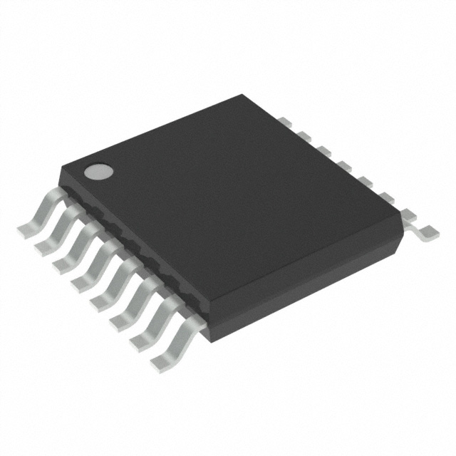
TMUX6212PWR

Why Choose Us?
Professional Platform
B2B & B2C purchasingDelivery at full speed
1-2 days deliveryWide variety
Original manufacturers365 days guarantee
Responsible quality
.png)


Tech Specifications
TMUX6212PWR Description
TMUX6212PWR Description
The TMUX6212PWR is a high-performance, 1:1 multiplexer/demultiplexer IC manufactured by Texas Instruments. This device is designed to provide excellent signal integrity and low power consumption in a compact 16-TSSOP package. With its low on-state resistance of 3.1 Ohms and fast switch times of 180ns and 220ns, the TMUX6212PWR is ideal for a wide range of applications in the electronics industry.
TMUX6212PWR Features
-
Technical Specifications: The TMUX6212PWR boasts a wide supply voltage range of ±4.5V to 18V for dual supply and 4.5V to 36V for single supply. It offers a low leakage current of 50pA, ensuring minimal power consumption in standby mode. The device also features excellent channel-to-channel matching with a maximum ΔRon of 100mOhm and low channel capacitance of 28pF and 45pF.
-
Performance Benefits: The TMUX6212PWR's low on-state resistance and fast switch times make it suitable for high-speed signal routing applications. Its low charge injection of 78pC minimizes signal distortion, while the -3dB bandwidth of 50MHz ensures reliable signal transmission.
-
Unique Features and Advantages: The TMUX6212PWR stands out from similar models with its REACH unaffected status, RoHS3 compliance, and EAR99 ECCN classification. These certifications ensure that the device meets strict environmental and regulatory requirements. Additionally, its moisture sensitivity level of 1 (unlimited) allows for flexible handling and storage options.
TMUX6212PWR Applications
The TMUX6212PWR is ideal for a variety of applications where high-speed signal routing and low power consumption are critical. Some specific use cases include:
-
Telecommunications: The device's fast switch times and low on-state resistance make it suitable for high-speed data transmission in telecommunications systems.
-
Industrial Control: The TMUX6212PWR's ability to handle a wide supply voltage range and low power consumption make it an excellent choice for industrial control systems.
-
Automotive: The device's robust performance and compliance with environmental and regulatory standards make it suitable for automotive applications, such as infotainment systems and sensor interfaces.
-
Medical Devices: The TMUX6212PWR's low leakage current and low charge injection make it ideal for medical devices that require precise signal routing and minimal power consumption.
Conclusion of TMUX6212PWR
The TMUX6212PWR is a versatile and high-performance multiplexer/demultiplexer IC that offers excellent signal integrity, low power consumption, and compliance with strict environmental and regulatory standards. Its unique features and advantages make it an ideal choice for a wide range of applications in the electronics industry, including telecommunications, industrial control, automotive, and medical devices.
FAQ
| Quantity | Unit Price | Ext. Price |
|---|---|---|
| 10+ | $2.71885 | $27.19 |
| 30+ | $2.40172 | $72.05 |
| 100+ | $2.07772 | $207.77 |
| 500+ | $1.93028 | $965.14 |
| 1000+ | $1.86685 | $1866.85 |
Not available to buy online? Want the lower wholesale price? Please Send RFQ to get best price, we will respond immediately


![STMicroelectronics_ST232ACD_VERY HIGH SPEED, ULTRA LOW POWER CONSUMPTION 5V POWERED RS-232 DRIVERS AND RECEIVERS, [0oC, 70oC] TEMPERATURE RANGE](https://media.ersaelectronics.com/static/20240425/stmicroelectronics/74ac257mtr.jpg?x-oss-process=image/format,webp/resize,p_25)


.png?x-oss-process=image/format,webp/resize,h_32)


