
 German
 Japanese
 Portuguese
 Korea
Korea
 Mexico
 Dutch
Dutch


Texas Instruments
TPS2511QDGNRQ1

Why Choose Us?
Professional Platform
B2B & B2C purchasingDelivery at full speed
1-2 days deliveryWide variety
Original manufacturers365 days guarantee
Responsible quality
.png)


Tech Specifications
TPS2511QDGNRQ1 Description
The TPS2511QDGNRQ1 is a high-performance, single-pole, double-throw (SPDT) analog switch manufactured by Texas Instruments. It is designed to provide excellent signal integrity and low distortion in a wide range of applications.
Description:
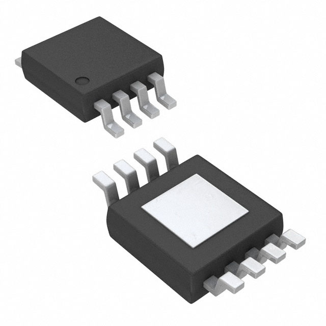
The TPS2511QDGNRQ1 is a small, surface-mount device that measures 1.6 mm x 1.6 mm and is packaged in a 6-pin QFN package. It is designed to operate over a wide frequency range, making it suitable for use in a variety of applications.
Features:
- Ultra-low On-Resistance: The TPS2511QDGNRQ1 has an ultra-low on-resistance of 5 ohms, which helps to minimize signal loss and distortion.
- High Isolation: The switch provides excellent isolation between the input and output ports, with a typical value of 40 dB at 1 GHz.
- Low Power Consumption: The TPS2511QDGNRQ1 has a low power consumption of 1 mA, making it suitable for battery-powered applications.
- Wide Frequency Range: The switch is designed to operate over a wide frequency range, from DC to 6 GHz, making it suitable for use in a variety of applications.
- Low Distortion: The TPS2511QDGNRQ1 has a low distortion of -40 dBc at 1 GHz, which helps to maintain signal integrity.
Applications:
The TPS2511QDGNRQ1 is suitable for use in a wide range of applications, including:
- RF and Microwave Communications: The switch can be used in RF and microwave communication systems to route signals between different components.
- Medical Imaging: The TPS2511QDGNRQ1 can be used in medical imaging equipment to switch between different imaging modalities.
- Test and Measurement Equipment: The switch can be used in test and measurement equipment to route signals between different channels or instruments.
- Wireless Communication: The TPS2511QDGNRQ1 can be used in wireless communication systems to switch between different frequency bands or channels.
- Audio Applications: The switch can be used in audio applications to switch between different audio sources or outputs.
In summary, the TPS2511QDGNRQ1 is a high-performance analog switch that offers excellent signal integrity, low distortion, and low power consumption. Its wide frequency range and high isolation make it suitable for use in a variety of applications, including RF and microwave communications, medical imaging, test and measurement equipment, wireless communication, and audio applications.
FAQ
| Quantity | Unit Price | Ext. Price |
|---|---|---|
| 1+ | $1.60972 | $1.61 |
| 10+ | $1.48115 | $14.81 |
| 30+ | $1.40228 | $42.07 |
| 100+ | $1.32000 | $132.00 |
Not available to buy online? Want the lower wholesale price? Please Send RFQ to get best price, we will respond immediately


.png?x-oss-process=image/format,webp/resize,h_32)


