

Texas Instruments
TPS61096ADSST
DC Switching Voltage Regulators

Not available to buy online? Want the lower wholesale price? Please Send RFQ to get best price, we will respond immediately


.png?x-oss-process=image/format,webp/resize,p_30)


TPS61096ADSST Description
TPS61096ADSST Description
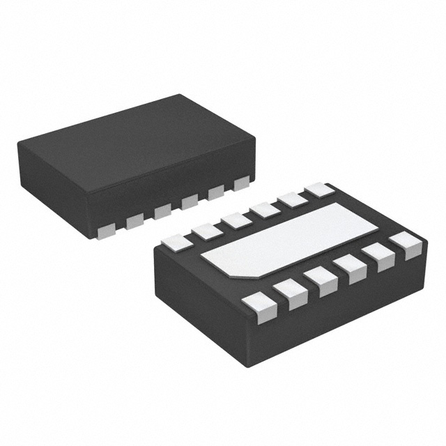
The TPS61096ADSST is a highly efficient, adjustable boost converter from Texas Instruments, designed to deliver up to 350mA of output current. This device is part of the Power Management Integrated Circuits (PMIC) category and is ideal for applications requiring a compact, high-performance power solution. The TPS61096ADSST operates over an input voltage range of 1.8V to 5.5V and can provide an adjustable output voltage from 4.5V to 28V, making it suitable for a wide range of electronic systems. The device is housed in a surface-mount 12-WSON package, which is available in tape and reel (TR) format, ensuring ease of integration into modern PCB designs.
TPS61096ADSST Features
- Adjustable Output Voltage: The TPS61096ADSST offers an adjustable output voltage range from 4.5V to 28V, providing flexibility to meet various application requirements.
- Wide Input Voltage Range: With an input voltage range of 1.8V to 5.5V, this boost converter can operate efficiently across a broad spectrum of power sources, enhancing its versatility.
- High Output Current: Capable of delivering up to 350mA of output current, the TPS61096ADSST ensures reliable power delivery to demanding loads.
- Positive Output Configuration: The device features a positive output configuration, simplifying circuit design and ensuring compatibility with most electronic systems.
- Efficient Power Conversion: Utilizing advanced power management techniques, the TPS61096ADSST achieves high conversion efficiency, minimizing power loss and heat generation.
- Compliance and Reliability: The TPS61096ADSST is REACH unaffected and RoHS3 compliant, ensuring it meets stringent environmental and safety standards. Additionally, its moisture sensitivity level (MSL) is 1 (unlimited), making it suitable for a variety of manufacturing environments.
- Boost Topology: The boost topology of the TPS61096ADSST allows for efficient voltage stepping up, making it ideal for applications where the input voltage is lower than the required output voltage.
TPS61096ADSST Applications
The TPS61096ADSST is well-suited for a variety of applications, including:
- Portable Electronics: Ideal for powering devices such as smartphones, tablets, and portable gaming consoles, where compact size and high efficiency are critical.
- Battery-Powered Systems: Suitable for applications that rely on battery power, such as wearable devices and IoT sensors, ensuring extended battery life and reliable performance.
- Communication Equipment: Can be used in various communication devices, including routers and modems, to provide stable power supply for critical components.
- Medical Devices: Applicable in medical equipment such as portable monitors and diagnostic tools, where reliability and efficiency are paramount.
Conclusion of TPS61096ADSST
The TPS61096ADSST from Texas Instruments stands out as a robust and versatile power management solution, offering a combination of adjustable output voltage, wide input voltage range, and high output current. Its compliance with environmental and safety standards, along with its efficient power conversion capabilities, make it a reliable choice for a wide range of applications. Whether powering portable electronics, battery-driven devices, or critical communication and medical equipment, the TPS61096ADSST delivers the performance and reliability needed to meet modern power management challenges.
Tech Specifications
TPS61096ADSST Documents
Download datasheets and manufacturer documentation for TPS61096ADSST
Mechanical Outline Drawing 150-V Output Low Power Boost Solution Using Coupled Transformer TPS61096 Unencrypted PSpice Transient Model Package (Rev. B) Export TINA-TI Transient Spice Model from WEBENCH (Rev. A) Related Parts


Shopping Guide


.png?x-oss-process=image/format,webp/resize,h_32)


©2025 ERSA Electronics Corporation.