
Texas Instruments
TS12A4517DR
Analog Switches, Multiplexers, Demultiplexers


.png?x-oss-process=image/format,webp/resize,p_30)


TS12A4517DR Description
TS12A4517DR Description
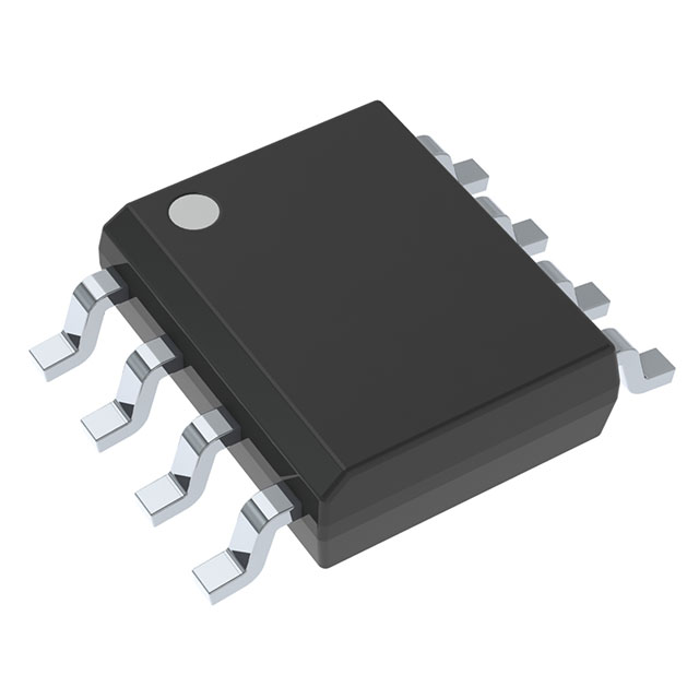
The TS12A4517DR is a high-performance, single-pole single-throw (SPST) analog switch designed by Texas Instruments. This device is ideal for applications requiring low on-state resistance and fast switching times. It features a maximum on-state resistance of 20 ohms and a leakage current of just 5nA, ensuring minimal power loss and high efficiency. The TS12A4517DR operates within a wide supply voltage range of ±1V to ±6V, making it suitable for various power supply configurations. Its channel capacitance is rated at 5.5pF for both source and drain, contributing to its high-frequency performance with a -3dB bandwidth of 464MHz. The switch time is impressively fast, with a turn-on time of 75ns and a turn-off time of 45ns, enabling rapid signal switching. The TS12A4517DR is packaged in an 8-pin small outline integrated circuit (SOIC) and is available in tape and reel format for surface mount applications. It is REACH unaffected and RoHS3 compliant, ensuring environmental safety and regulatory compliance.
TS12A4517DR Features
- Low On-State Resistance: The TS12A4517DR boasts a maximum on-state resistance of 20 ohms, ensuring minimal voltage drop and power dissipation, which is crucial for high-current applications.
- Fast Switching Times: With a turn-on time of 75ns and a turn-off time of 45ns, the TS12A4517DR offers rapid signal switching, making it suitable for high-speed applications.
- Wide Operating Voltage Range: The device operates within a dual supply voltage range of ±1V to ±6V, providing flexibility in power supply design.
- Low Leakage Current: The maximum leakage current of 5nA ensures minimal power loss, making the TS12A4517DR ideal for low-power and battery-operated applications.
- High-Frequency Performance: The -3dB bandwidth of 464MHz allows the TS12A4517DR to handle high-frequency signals with minimal attenuation.
- Low Channel Capacitance: With a channel capacitance of 5.5pF for both source and drain, the TS12A4517DR minimizes signal distortion and delay.
- Environmental Compliance: The TS12A4517DR is REACH unaffected and RoHS3 compliant, ensuring it meets the highest environmental standards.
- Surface Mount Packaging: The 8-pin SOIC package and tape and reel format make the TS12A4517DR ideal for automated assembly processes.
TS12A4517DR Applications
The TS12A4517DR is well-suited for a variety of applications due to its high performance and flexibility. Some specific use cases include:
- High-Speed Signal Routing: The fast switching times and high-frequency performance make the TS12A4517DR ideal for routing high-speed digital and analog signals in communication systems.
- Battery-Powered Devices: The low leakage current and low on-state resistance ensure minimal power consumption, making the TS12A4517DR suitable for battery-operated devices.
- Audio Signal Processing: The low channel capacitance and high bandwidth allow for high-fidelity audio signal switching without distortion.
- Medical Equipment: The TS12A4517DR's low leakage current and environmental compliance make it suitable for sensitive medical applications where reliability and safety are paramount.
- Automotive Electronics: The wide operating voltage range and robust performance ensure reliable operation in the demanding conditions of automotive electronics.
Conclusion of TS12A4517DR
The TS12A4517DR from Texas Instruments is a versatile and high-performance analog switch that stands out in its category. Its low on-state resistance, fast switching times, and wide operating voltage range make it suitable for a variety of applications, from high-speed signal routing to battery-powered devices. The device's environmental compliance and surface mount packaging further enhance its appeal for modern electronics manufacturing. Whether in communication systems, medical equipment, or automotive electronics, the TS12A4517DR offers reliable performance and efficiency, making it a preferred choice for engineers and designers.
Tech Specifications
TS12A4517DR Documents
Download datasheets and manufacturer documentation for TS12A4517DR
 Mechanical Outline Drawing
  Product Change Notification (PDF)
  TS12A4517DR Symbol & Footprint by SnapMagic
  Analog Switch Guide (Rev. D)
  TS12A4517 PSpice Model
 Shopping Guide


.png?x-oss-process=image/format,webp/resize,h_32)


