
 German
 Japanese
 Portuguese
 Korea
Korea
 Mexico
 Dutch
Dutch


Texas Instruments
TS3DV421DGVR
684-TS3DV421DGVR

PDF Datasheet
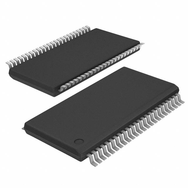
Multi-Channel Differential Switch/Multiplexer Targeting DVI/HDMI Applications 48-TVSOP -40 to 85
6 Weeks
Why Choose Us?
Professional Platform
B2B & B2C purchasingDelivery at full speed
1-2 days deliveryWide variety
Original manufacturers365 days guarantee
Responsible quality
.png)


Tech Specifications
Bandwidth
1.9GHz
Package/Case
TFSOP
Control Interface
SERIAL
Data Rate
3800Mbps
Dual Supply Voltage
1.65V
Lead Free
Lead Free
Max Dual Supply Voltage
1.8V
Min Dual Supply Voltage
1.5V
TS3DV421DGVR Description
Video Switch IC Serial DVI 1.0, HDMI 1.3 48-TVSOP Package
FAQ
What is the standard lead time for TS3DV421DGVR?
The standard lead time for TS3DV421DGVR is 6 Weeks.
Does TS3DV421DGVR have quantity-based pricing?
What operating temperature range does TS3DV421DGVR support?
Are there related or alternative parts for TS3DV421DGVR?
Is TS3DV421DGVR currently in stock?
Quick Quote
ADD TO RFQ LIST
Not available to buy online? Want the lower wholesale price? Please Send RFQ to get best price, we will respond immediately
QUICK RFQ


.png?x-oss-process=image/format,webp/resize,h_32)


