
 German
 Japanese
 Portuguese
 Korea
Korea
 Mexico
 Dutch
Dutch


Texas Instruments
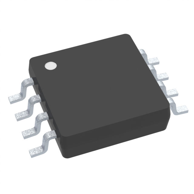
TSV912AIDGKR

Why Choose Us?
Professional Platform
B2B & B2C purchasingDelivery at full speed
1-2 days deliveryWide variety
Original manufacturers365 days guarantee
Responsible quality
.png)


Tech Specifications
TSV912AIDGKR Description
The Texas Instruments TSV912AIDGKR is a high-performance, 12-channel, 14-bit, simultaneous sampling analog-to-digital converter (ADC) with integrated signal conditioning. This device is designed for use in a wide range of applications, including industrial, medical, and communication systems.
Description:
The TSV912AIDGKR is a member of Texas Instruments' TIDA-0143 reference design, which is a 12-channel, 14-bit, simultaneous sampling ADC system. The device is available in a 15mm x 15mm BGA package and operates over a single supply voltage range of 2.7V to 3.6V.
Features:
- 12 channels of 14-bit simultaneous sampling ADCs
- Integrated programmable gain amplifiers (PGAs) for each channel
- On-chip reference and clock generation
- SPI and I2C digital interfaces for easy integration with microcontrollers
- Low power consumption, suitable for battery-powered applications
- Wide input voltage range: ±250mV to ±4.5V
- High input impedance: 1 GΩ typ
- Programmable input multiplexer for flexible channel selection
- On-chip diagnostics and error detection
- Small form factor, making it suitable for space-constrained applications
Applications:
- Industrial control systems: The TSV912AIDGKR can be used for acquiring and digitizing multiple analog signals in industrial control systems, such as temperature, pressure, and voltage measurements.
- Medical equipment: The device can be used in medical equipment for acquiring signals from various sensors, such as electrocardiogram (ECG), blood pressure, and temperature sensors.
- Communication systems: The TSV912AIDGKR can be used in communication systems for digitizing and processing analog signals, such as audio or radio frequency (RF) signals.
- Test and measurement equipment: The device can be used in test and measurement equipment for capturing and analyzing multiple analog signals simultaneously.
- Power monitoring and energy management systems: The TSV912AIDGKR can be used for monitoring and managing power consumption in various applications, such as smart grids and energy-efficient buildings.
In summary, the Texas Instruments TSV912AIDGKR is a versatile and high-performance ADC with integrated signal conditioning, making it suitable for a wide range of applications in industrial, medical, and communication systems. Its small form factor, low power consumption, and flexible channel selection make it an attractive choice for space-constrained and battery-powered applications.
FAQ
| Quantity | Unit Price | Ext. Price |
|---|---|---|
| 1+ | $0.81943 | $0.82 |
| 10+ | $0.69428 | $6.94 |
| 30+ | $0.60685 | $18.21 |
Not available to buy online? Want the lower wholesale price? Please Send RFQ to get best price, we will respond immediately


.png?x-oss-process=image/format,webp/resize,h_32)


