
Texas Instruments
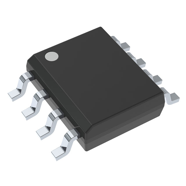
TSV912AIDR
OP Amps, Buffer Amps ICs


.png?x-oss-process=image/format,webp/resize,p_30)


TSV912AIDR Description
TSV912AIDR Description
The TSV912AIDR is a high-performance, dual-channel operational amplifier (op-amp) designed by Texas Instruments. This general-purpose amplifier is known for its exceptional performance and versatility, making it suitable for a wide range of applications. With a supply voltage range of 2.5 V to 5.5 V, the TSV912AIDR can operate in various power supply environments. It offers a gain bandwidth product of 8 MHz and a -3dB bandwidth of 80 kHz, ensuring fast response times and high-frequency performance. The slew rate of 4.5 V/µs further enhances its ability to handle rapid changes in input signals.
TSV912AIDR Features
- Low Input Bias Current: The TSV912AIDR boasts an ultra-low input bias current of 1 pA, which is crucial for maintaining signal integrity in high-impedance applications.
- Low Voltage Operation: With a minimum supply voltage of 2.5 V, the TSV912AIDR is well-suited for battery-powered devices and other low-voltage applications.
- High Output Current: Each channel can deliver up to 50 mA, making it suitable for driving heavy loads.
- Low Input Offset Voltage: The input offset voltage of 300 µV ensures high accuracy and precision in signal amplification.
- RoHS Compliance: The TSV912AIDR is compliant with the RoHS3 directive, making it an environmentally friendly choice for electronic designs.
- REACH Unaffected Status: This op-amp is not affected by the REACH regulation, ensuring uninterrupted supply and compliance with European chemical regulations.
TSV912AIDR Applications
The TSV912AIDR is ideal for a variety of applications due to its combination of performance and flexibility:
- Audio Amplification: Its high slew rate and low distortion make it suitable for audio applications, such as preamplifiers and audio mixers.
- Data Acquisition Systems: The low input bias current and low noise characteristics are beneficial for accurate signal conditioning in data acquisition systems.
- Sensor Signal Conditioning: The TSV912AIDR can be used to amplify and filter signals from sensors in industrial and automotive applications.
- Medical Equipment: Its low noise and high precision make it suitable for amplifying in medical devices.
Conclusion of TSV912AIDR
The TSV912AIDR from Texas Instruments stands out as a robust, dual-channel op-amp with a wide supply voltage range, low input bias current, and high slew rate. Its compliance with RoHS and unaffected status by REACH regulations make it an environmentally conscious choice. With its versatile performance, the TSV912AIDR is an excellent choice for applications requiring high precision and fast response times, such as audio processing, data acquisition, and sensor signal conditioning.
Tech Specifications
TSV912AIDR Documents
Download datasheets and manufacturer documentation for TSV912AIDR
 LMx/LMVx/TLVx/TSVx 20/Jun/2022
  TSV911, 912, 914 Datasheet
  TSV911, 912, 914 Datasheet
  Mult Dev 27/Jul/2023 Mult Dev Wire Dia Chg 20/Sep/2018
 Shopping Guide


.png?x-oss-process=image/format,webp/resize,h_32)


