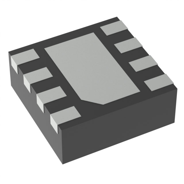
Texas Instruments_TSV912AIDSGR

Texas Instruments
TSV912AIDSGR  
OP Amps, Buffer Amps ICs

Texas Instruments
TSV912AIDSGR
687-TSV912AIDSGR
Ersa
Texas Instruments-TSV912AIDSGR-datasheets-2920048.pdf
IC OPAMP GP 2 CIRCUIT 8WSON
In Stock : 4710

Not available to buy online? Want the lower wholesale price? Please Send RFQ to get best price, we will respond immediately

QUICK RFQ
ADD TO RFQ LIST
ersa FreeSample ersa flow
  • Quantity
  • Unit Price
  • Ext. Price
    • 1+
    • $0.70546
    • $0.71
    • 10+
    • $0.58457
    • $5.85
    • 30+
    • $0.52495
    • $15.75
    • 100+
    • $0.46534
    • $46.53
    • 500+
    • $0.42890
    • $214.45
    ADD TO CART
    QUICK ORDER
    $0.70546    $0.71
    ISO9001
    Quality Policy
    ISO45001
    ISO14001

    TSV912AIDSGR Description

    The TSV912AIDSGR is a high-performance, single-chip digital signal processor (DSP) from Texas Instruments. It is designed for a wide range of applications, including industrial control, medical imaging, and telecommunications.

    Description:

    The TSV912AIDSGR is a member of Texas Instruments' TMS320C6000 DSP family. It is a high-performance, fixed-point DSP that offers a combination of high processing power, low power consumption, and advanced features. The device is available in a small, 14mm x 14mm, 208-ball BGA package.

    Features:

    1. High processing power: The TSV912AIDSGR features a high-performance CPU with a clock speed of up to 1 GHz, providing up to 8192 MIPS (million instructions per second).
    2. Low power consumption: The device offers low power consumption, making it suitable for battery-powered applications.
    3. Advanced features: The TSV912AIDSGR includes a range of advanced features, including a 64-bit CPU, a 64-bit memory interface, and a 64-bit external bus interface.
    4. Memory: The device includes up to 1 MB of on-chip memory, including 512 KB of Level 1 program and data memory, and up to 512 KB of Level 2 memory.
    5. Connectivity: The TSV912AIDSGR includes a range of connectivity options, including USB, Ethernet, and serial communication interfaces.

    Applications:

    The TSV912AIDSGR is suitable for a wide range of applications, including:

    1. Industrial control: The device's high processing power and low power consumption make it ideal for industrial control applications, such as motor control, robotics, and automation.
    2. Medical imaging: The TSV912AIDSGR can be used in medical imaging applications, such as ultrasound and CT scanners, to process large amounts of data quickly and accurately.
    3. Telecommunications: The device's connectivity options and high processing power make it suitable for telecommunications applications, such as voice over IP (VoIP) and signal processing.
    4. Video processing: The TSV912AIDSGR can be used in video processing applications, such as video encoding and decoding, image and video analysis, and video surveillance.
    5. Audio processing: The device's advanced signal processing capabilities make it suitable for audio processing applications, such as audio encoding and decoding, and voice recognition.

    In summary, the TSV912AIDSGR is a high-performance DSP from Texas Instruments that offers a combination of high processing power, low power consumption, and advanced features. It is suitable for a wide range of applications, including industrial control, medical imaging, telecommunications, video processing, and audio processing.

    Tech Specifications

    Number of Channels per Chip
    Unit Weight
    Power Supply Type
    Typical Output Current (mA)
    Rail-to-rail
    Product
    PPAP
    Gain Bandwidth Product
    Automotive
    RoHS
    THD plus Noise
    REACH Status
    Input common mode headroom (to negative supply) (typ) (V)
    Operating temperature range (°C)
    Supplier Temperature Grade
    Current - Supply
    Output swing headroom (to negative supply) (typ) (V)
    Standard Package Name
    Shut Down Support
    Mounting
    Minimum Single Supply Voltage (V)
    Iout (typ) (A)
    Manufacturer Type
    Package
    Minimum CMRR (dB)
    Maximum Quiescent Current (mA)
    Total supply voltage (+5 V = 5, ±5 V = 10) (max) (V)
    GBW (typ) (MHz)
    3 dB Bandwidth
    en - Input Voltage Noise Density
    Output Type
    Vos - Input Offset Voltage
    Minimum CMRR Range (dB)
    Typical Gain Bandwidth Product (MHz)
    Development Kit
    Package Height
    Maximum Operating Temperature
    Ib - Input Bias Current
    RoHS Status
    Number of channels
    Iq per channel (typ) (mA)
    Minimum Operating Temperature
    Voltage - Input Offset
    Type
    Vos (offset voltage at 25°C) (max) (mV)
    Output Current per Channel
    Part Status
    Input Offset Voltage Drift (uV/°C)
    Lead finish / Ball material
    Number of Circuits
    Package Width
    GBP - Gain Bandwidth Product
    Voltage - Supply Span (Max)
    Maximum Input Offset Voltage (mV)
    Typical Output Resistance (Ohm)
    Product Status
    Current - Input Bias
    Rail to Rail
    Supplier Package
    Package / Case
    Number of Channels
    Typical Voltage Gain (dB)
    Typical Input Bias Current (uA)
    EU RoHS
    Carrier
    Amplifier Type
    Maximum Dual Supply Voltage (V)
    Input common mode headroom (to positive supply) (typ) (V)
    Moisture Sensitivity Level (MSL)
    Typical Input Noise Voltage Density (nV/rtHz)
    Operating Temperature
    Architecture
    Typical Slew Rate (V/us)
    Output swing headroom (to positive supply) (typ) (V)
    ECCN
    MSL rating / Peak reflow
    Mounting Type
    Pin Count
    In - Input Noise Current Density
    Ios - Input Offset Current
    Minimum PSRR (dB)
    Shutdown
    Voltage - Supply Span (Min)
    Lead Shape
    HTSUS
    Pins
    Current - Output / Channel
    USHTS
    PCB changed
    HTS
    Rating
    ECCN (US)
    Total supply voltage (+5 V = 5, ±5 V = 10) (min) (V)
    Supplier Device Package
    Supply Voltage - Min
    Minimum Operating Temperature (°C)
    Maximum Operating Temperature (°C)
    Operating Supply Current
    SR - Slew Rate
    Mfr
    Features
    CMRR (typ) (dB)
    Supply Voltage - Max
    Offset drift (typ) (µV/°C)
    Mounting Style
    Input Type
    Typical Noninverting Input Current Noise Density (pA/rtHz)
    Slew Rate
    Package Length
    Minimum Dual Supply Voltage (V)
    Vn at 1 kHz (typ) (nV√Hz)
    CMRR - Common Mode Rejection Ratio
    REACH
    Series
    Maximum Single Supply Voltage (V)
    Slew rate (typ) (V/µs)
    Typical Settling Time (ns)
    Base Product Number

    TSV912AIDSGR Documents

    Download datasheets and manufacturer documentation for TSV912AIDSGR

    Ersa TSV911, 912, 914 Datasheet      
    Ersa TSV911, 912, 914 Datasheet      

    Shopping Guide

    Payment Methods
    Payment Methods include Prepayment TT (bank transfer), Western Union, and PayPal. Customers are responsible for shipping costs, bank charges, customs duties and taxes.
    Shipping Rate
    Shipments are made once a day around 5pm, excluding Sundays. Once shipped, the estimated delivery time is usually 5-7 business days, depending on the courier you choose.
    Delivery Methods
    Provide DHL, FedEx, UPS, EMS, SF Express and Registered Airmail International Delivery Service