
 German
 Japanese
 Portuguese
 Korea
Korea
 Mexico
 Dutch
Dutch


Texas Instruments
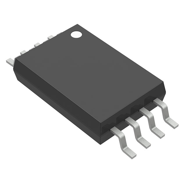
TSV912AIPWR

Why Choose Us?
Professional Platform
B2B & B2C purchasingDelivery at full speed
1-2 days deliveryWide variety
Original manufacturers365 days guarantee
Responsible quality
.png)


Tech Specifications
TSV912AIPWR Description
TSV912AIPWR Description
The TSV912AIPWR is a high-performance, dual-channel operational amplifier (op-amp) designed and manufactured by Texas Instruments. This general-purpose amplifier is known for its robust performance and versatility, making it suitable for a wide range of applications. With a supply voltage span ranging from 2.5 V to 5.5 V and a gain bandwidth product of 8 MHz, the TSV912AIPWR delivers exceptional performance in various electronic systems.
TSV912AIPWR Features
- Voltage - Supply Span (Max): 5.5 V
- Gain Bandwidth Product: 8 MHz
- Product Status: Active
- Current - Input Bias: 1 pA
- REACH Status: REACH Unaffected
- Manufacturer: Texas Instruments
- Amplifier Type: General Purpose
- RoHS Status: ROHS3 Compliant
- Moisture Sensitivity Level (MSL): 2 (1 Year)
- ECCN: EAR99
- -3db Bandwidth: 80 kHz
- Slew Rate: 4.5V/µs
- Mounting Type: Surface Mount
- Current - Supply: 550µA (x2 Channels)
- Voltage - Input Offset: 300 µV
- Voltage - Supply Span (Min): 2.5 V
- HTSUS: 8542.33.0001
- Package: Tape & Reel (TR)
- Number of Circuits: 2
- Current - Output / Channel: 50 mA
- Base Product Number: TSV912
TSV912AIPWR Applications
The TSV912AIPWR is ideal for applications that require high precision and performance in a compact form factor. Some specific use cases include:
- Audio Amplification: Due to its low input bias current and high slew rate, the TSV912AIPWR is well-suited for audio applications, providing clear and distortion-free audio signals.
- Sensor Signal Conditioning: The TSV912AIPWR's low input offset voltage and low noise make it an excellent choice for conditioning signals from sensors in industrial and automotive applications.
- Data Acquisition Systems: In data acquisition systems, the TSV912AIPWR's high bandwidth and low distortion enable accurate signal processing and analysis.
- Communication Systems: The TSV912AIPWR's ability to handle a wide range of supply voltages and its low power consumption make it suitable for communication systems, such as modems and transceivers.
Conclusion of TSV912AIPWR
The TSV912AIPWR from Texas Instruments is a versatile and high-performance dual-channel op-amp that offers a unique combination of technical specifications and performance benefits. Its low input bias current, high slew rate, and wide supply voltage range make it an ideal choice for a variety of applications, including audio amplification, sensor signal conditioning, data acquisition systems, and communication systems. With its RoHS compliance and REACH unaffected status, the TSV912AIPWR is not only a powerful solution but also an environmentally responsible choice for electronic design engineers.
FAQ
| Quantity | Unit Price | Ext. Price |
|---|---|---|
| 10+ | $0.50915 | $5.09 |
| 30+ | $0.45428 | $13.63 |
| 100+ | $0.38743 | $38.74 |
| 500+ | $0.35657 | $178.28 |
| 1000+ | $0.33772 | $337.72 |
Not available to buy online? Want the lower wholesale price? Please Send RFQ to get best price, we will respond immediately


.png?x-oss-process=image/format,webp/resize,h_32)


