
Texas Instruments
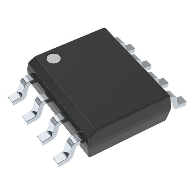
UCC5390SCDR
Isolators - Gate Drivers


- 1+
- $2.44591
- $2.45
- 10+
- $2.10146
- $21.01
- 30+
- $1.88784
- $56.64
- 100+
- $1.66759
- $166.76
- 500+
- $1.56823
- $784.12

.png?x-oss-process=image/format,webp/resize,p_30)


UCC5390SCDR Description
The UCC5390SCDR is a high-performance, monolithic, step-down switching regulator from Texas Instruments. It is designed to provide efficient and stable voltage regulation for a wide range of applications. Here is a description of the UCC5390SCDR, along with its features and applications:
Description:
The UCC5390SCDR is a step-down (buck) switching regulator that uses a fixed-frequency, current-mode control scheme to provide efficient power conversion. It is available in a compact, thermally enhanced, SC70-5 package, making it suitable for space-constrained applications.
Features:
- Wide input voltage range: The UCC5390SCDR can operate with input voltages from 4.75V to 40V, making it suitable for a variety of power supply sources.
- High efficiency: The regulator offers high efficiency levels, with typical values above 90%, depending on the input voltage and output current requirements.
- Low quiescent current: The UCC5390SCDR has a low quiescent current of 3.5μA, which is ideal for battery-powered applications where minimizing power consumption is crucial.
- Fixed 1.25MHz switching frequency: The fixed switching frequency allows for simple external component selection and reduces the need for frequency compensation.
- Wide output voltage range: The regulator can provide output voltages from 0.9V to 40V, making it suitable for a broad range of applications.
- Current-sense feedback: The UCC5390SCDR features a current-sense feedback pin that allows for accurate current monitoring and protection.
- Overcurrent protection: The regulator includes overcurrent protection to prevent damage to the output in case of excessive current draw.
- Thermal shutdown: The UCC5390SCDR has a thermal shutdown feature that protects the device from overheating.
Applications:
- Portable devices: Due to its high efficiency and low quiescent current, the UCC5390SCDR is well-suited for battery-powered applications such as smartphones, tablets, and wearable devices.
- Power supplies: The regulator can be used in compact power supply designs for a variety of electronic devices, including laptops, routers, and IoT devices.
- LED lighting: The UCC5390SCDR can be used for driving LED lighting applications, providing efficient power conversion and dimming control.
- Medical devices: The regulator's high efficiency and low noise make it suitable for use in battery-powered medical devices, such as hearing aids and portable medical instruments.
- Industrial control: The UCC5390SCDR can be used in industrial control applications where stable and efficient power regulation is required.
In summary, the Texas Instruments UCC5390SCDR is a versatile, high-performance step-down switching regulator that offers a wide input voltage range, high efficiency, and a fixed switching frequency. Its compact size and low quiescent current make it suitable for a variety of applications, including portable devices, power supplies, LED lighting, medical devices, and industrial control systems.
Tech Specifications
UCC5390SCDR Documents
Download datasheets and manufacturer documentation for UCC5390SCDR
 Mult Dev Material Chg 8/Jul/2021
  UCC53x0 Datasheet
  Marking Standardization 18/May/2023
  UCC53x0 Datasheet
  UCC5310/UCC5320/UCC5350/UCC5390 08/Jan/2019
 Shopping Guide


.png?x-oss-process=image/format,webp/resize,h_32)


