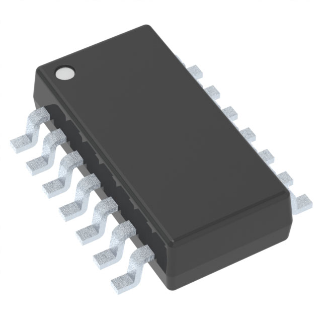
TPSF12C1-Q1
TPSF12C1-Q1 is a high-performance power MOSFET from Texas Instruments, designed for efficient switching applications in automotive and industrial systems. It features a low on-resistance of 12 mΩ at VGS = 10 V, enabling minimal conduction losses and high power efficiency. The device is optimized for operation with a maximum drain-source voltage (VDS) of 60 V, making it suitable for a wide range of voltage conditions in modern power conversion circuits.
This MOSFET is built using advanced trench technology to enhance gate charge characteristics and reduce switching losses, especially under high-frequency operation. Its total gate charge (QG) is minimized to improve switching speed while maintaining robustness against electromagnetic interference (EMI). The device also includes an integrated body diode with low forward voltage drop, which supports efficient freewheeling current paths in inductive loads such as motors or DC-DC converters.
The TPSF12C1-Q1 is qualified to AEC-Q101 standards, ensuring reliability in harsh automotive environments, including extreme temperature variations, vibration, and thermal cycling. It operates reliably over a junction temperature range from -40°C to +175°C, making it ideal for engine control units, battery management systems, and electric vehicle powertrains. Enhanced thermal performance is achieved through a direct bond copper (DBC) package structure that improves heat dissipation and reduces thermal resistance.
Functionally, the device supports both synchronous rectification and buck/boost converter topologies, offering flexibility in power supply design. Its fast turn-on and turn-off times enable high-frequency switching up to several hundred kHz, contributing to smaller passive components and overall system miniaturization. Additionally, the MOSFET provides excellent avalanche energy capability, enhancing protection against inductive kickback events common in motor control and relay driver circuits.
Designed for ease of integration, the TPSF12C1-Q1 comes in a compact TO-220-3L package, compatible with standard PCB assembly processes. It also offers inherent protection against parasitic latch-up due to its unique cell structure and layout, improving long-term operational safety. With low gate threshold voltage (VGS(th) = 1.2 V typical), it can be driven directly by microcontrollers or digital logic without requiring additional level-shifting circuitry.
Related Parts
| Part # | Manufacturer | Description | Availability | Pricing | Quantity |
|---|---|---|---|---|---|
 TPSF12C1QDYYRQ1Active Filters | Texas Instruments | AUTOMOTIVE COMMON-MODE ACTIVE EM | 2399 | 1+: $1.62610 10+: $1.34734 100+: $1.25442 1000+: $1.20796 |


.png?x-oss-process=image/format,webp/resize,h_32)


