
 German
 Japanese
 Portuguese
 Korea
Korea
 Mexico
 Dutch
Dutch


Memory Chips: Materials, Applications, Types, and On-Chip Memory Explained

Most memory chips are built on high-purity monocrystalline silicon wafers with metal interconnects, dielectric layers, and doped transistor regions.
Memory ICs are used in RAM modules, SSDs, smartphones, servers, routers, automotive ECUs, industrial controls, and embedded systems.
Common memory chips include DRAM, SRAM, NAND flash, NOR flash, ROM, EEPROM, CMOS memory, and on-chip memory blocks.
What Are Memory Chips Made Of?
Foundation: From a Grain of Sand to a Perfect Silicon Wafer
Memory chips are built on an extremely pure semiconductor material: silicon (Si). Although silicon is ultimately derived from silica-rich materials such as sand, chips are not made directly from ordinary sand. Instead, silicon must be purified, crystallized, sliced, polished, and processed through highly complex semiconductor manufacturing techniques.
- Material: High-purity monocrystalline silicon.
- Form: A wafer, which is a thin circular disc similar in shape to an optical disc.
- Function: The wafer acts as the physical carrier and foundation of the chip. All circuits are built on this nearly perfect silicon crystal.
Bridge: The “Copper Roads” Connecting Billions of Transistors
There are billions of tiny transistors inside a memory chip. To work together, they must be connected by extremely fine “wires.” These microscopic interconnects are made from specific metal materials:
- Main conductive material: Copper (Cu). Copper has become the mainstream choice because of its excellent electrical conductivity.
- Local connection material: Tungsten (W). Tungsten is commonly used for vertical connections or contact holes because of its stability.
- Early or special-purpose material: Aluminum (Al). Aluminum was the main interconnect material in earlier chips, although it is now used less widely in advanced processes.
Core: Special Materials for Building Data “Cages” and Highways
If the wafer is compared to a city, memory cells are like buildings with different functions. To build these structures, engineers use a variety of special materials. The material combination varies depending on the type of memory chip.
| Chip Type | Core Material Combination | Function and Metaphor |
|---|---|---|
| DRAM Such as memory modules |
|
The capacitor dielectric is like an ultra-thin insulating film. Its high dielectric constant allows it to store more charge in a very small space. The electrode acts like the plate of a capacitor. |
| 3D NAND Flash Used in SSDs and other storage devices |
Option 1: Floating-gate type
|
In the floating-gate approach, electrons are “locked” inside an independent polysilicon cage, similar to a tiny Faraday cage. In the charge-trap approach, electrons are captured in many small, discrete traps inside the silicon nitride layer. |
| SRAM Such as CPU cache |
Standard silicon substrates, polysilicon or metal gate structures, and transistor interconnects. | SRAM does not depend on capacitor-like storage materials. Its six-transistor flip-flop circuit stores data through stable transistor states. |
Future: Exploring Cutting-Edge Materials with New Physical Mechanisms
Scientists are not stopping at today’s memory technologies. They are exploring a new generation of memory devices that use novel physical principles to store data. These technologies may one day combine the speed of SRAM with the non-volatility of flash memory.
| Memory Type | Core Material Combination | Basic Principle |
|---|---|---|
| MRAM Magnetoresistive Random Access Memory |
|
MRAM stores data using the magnetic moment direction of magnetic materials, similar to the polarity of a tiny magnet. The resistance changes depending on the direction of the magnetic moments. |
| ReRAM Resistive Random Access Memory |
|
ReRAM records data by applying voltage to form or break conductive filaments inside the material, thereby changing its resistance. |
Auxiliary Materials: The Indispensable “Glue” and Protective Shield
In addition to the core functional materials above, memory chips also rely on many auxiliary materials that are essential for construction, insulation, pattern transfer, protection, and electrical connection.
| Functional Category | Common Materials | Function |
|---|---|---|
| Dielectric / Isolation | Silicon dioxide (SiO₂) and other insulating layers | Isolate different circuit layers inside the chip, prevent short circuits and signal interference, and help form transistor gates. |
| Dopants | Boron, phosphorus, arsenic | Precisely injected into silicon to change its conductivity and form key transistor regions such as the source and drain. |
| Photoresist | Photosensitive polymer materials | Used as a temporary template during manufacturing to accurately transfer circuit patterns onto the wafer. |
| Packaging Protection | Epoxy resin, ceramics, gold bonding wires, solder balls, and related materials | Provide physical protection, heat dissipation, electrical connection, and resistance to electromagnetic interference for fragile chips. |
What Are Memory Chips Used For?
A memory chip is a core component of electronic devices, mainly used for storing data. Depending on whether data is lost after power is removed, memory chips can be divided into two major categories. Their purposes are also significantly different.
Volatile Memory Chips
Volatile memory loses data immediately after power is turned off, but it is extremely fast. It is mainly used as working memory for devices.
- Computer and phone memory
- Server and cloud computing memory
- Graphics card memory
- CPU and GPU cache
- Network equipment buffering
Non-Volatile Memory Chips
Non-volatile memory keeps data even after power is turned off. It is used to store information that must be retained for a long time.
- SSDs and embedded storage
- USB flash drives and memory cards
- Firmware and boot code
- Industrial and automotive data logging
- Security keys and certificates
DRAM: Dynamic Random Access Memory
DRAM is the most common type of system memory. It is used in computers, smartphones, servers, cloud computing systems, AI training platforms, high-performance computing systems, and graphics cards.
SRAM: Static Random Access Memory
SRAM is extremely fast, but it is expensive and usually has a small capacity. It is commonly used in CPU cache, GPU cache, networking chips, routers, switches, and high-speed packet buffering systems.
NAND Flash Memory
NAND flash memory is currently the mainstream high-capacity storage medium. It is used in SSDs, smartphones, tablets, digital cameras, USB drives, memory cards, dashcams, autonomous driving data recorders, and industrial robots.
NOR Flash Memory
NOR flash memory can support direct code execution. It reads quickly, but writes more slowly and usually has a smaller capacity. It is widely used for BIOS, router firmware, IoT startup code, smartwatch operating systems, 5G base station configurations, and automotive ECU programs.
ROM, PROM, and EEPROM
Other specialized memory chips such as ROM, PROM, and EEPROM are used for firmware, calibration parameters, fixed factory programs, keyboard controllers, battery management chips, encryption keys, digital certificates, bank cards, and electronic passports.
In summary: DRAM is responsible for “running” programs and providing a large temporary workspace for the CPU and GPU. NAND flash is responsible for “storage,” permanently keeping user data and files. NOR flash is responsible for “booting,” storing the most basic startup programs.
What Data Is Stored in a CMOS Memory Chip?
The data stored in a CMOS memory chip mainly includes computer hardware configuration information and BIOS/UEFI setting parameters. It acts like a small archive for the motherboard. If the CMOS battery runs out of power, many customized settings may be cleared.
System Time and Date
CMOS memory stores the current year, month, day, hour, minute, and second. Because the motherboard battery continuously powers the real-time clock and related settings, the system time can still be recorded even when the computer is turned off.
Hardware Configuration Parameters
CMOS-related settings record storage device information, processor and memory information, I/O interface configuration, onboard audio and network status, serial and parallel port resources, IRQ settings, I/O addresses, and older display standards such as EGA or VGA.
System Startup and Performance Settings
CMOS settings may include boot device sequence, CPU frequency settings, bus speed, multiplier settings, and power management options. These settings help determine how the computer starts and how hardware operates.
Security and Power Management
CMOS memory may also store security-related BIOS settings, such as supervisor passwords and user passwords. Power management settings, including ACPI behavior, standby, sleep, and wake-up modes, can also be configured through BIOS/UEFI settings.
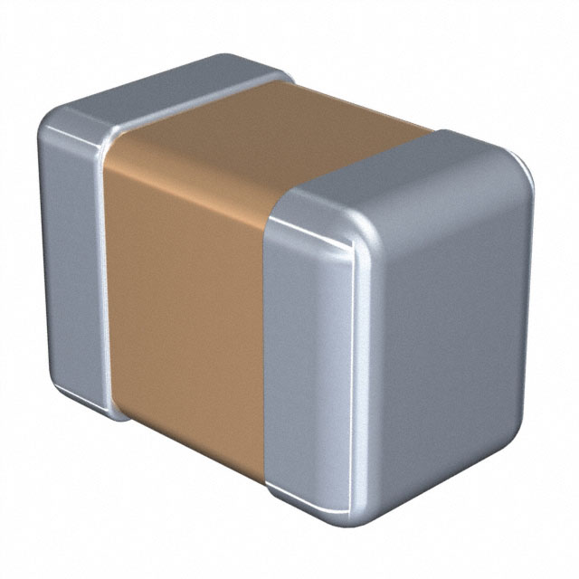
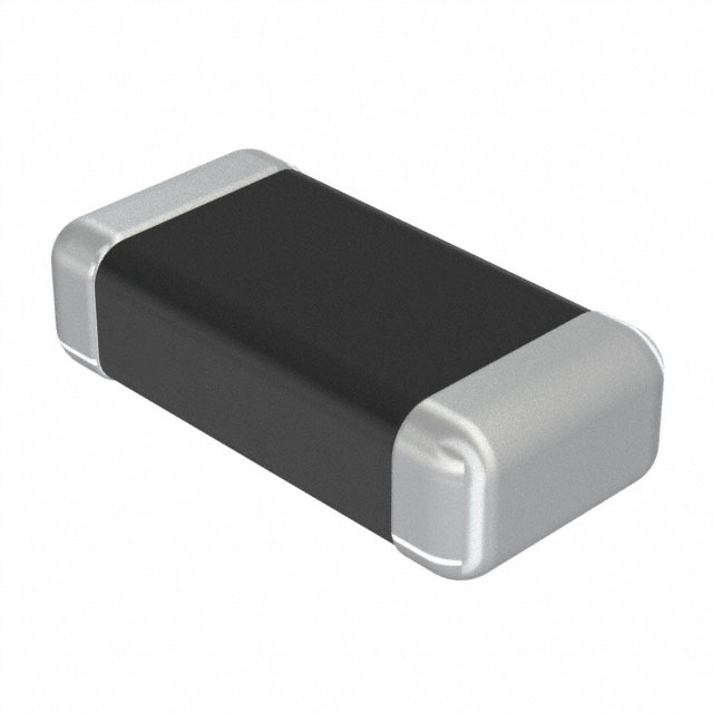
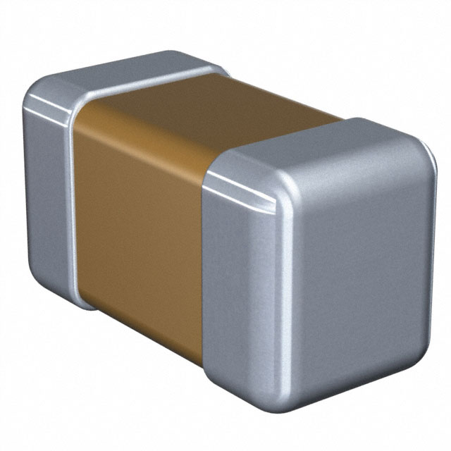
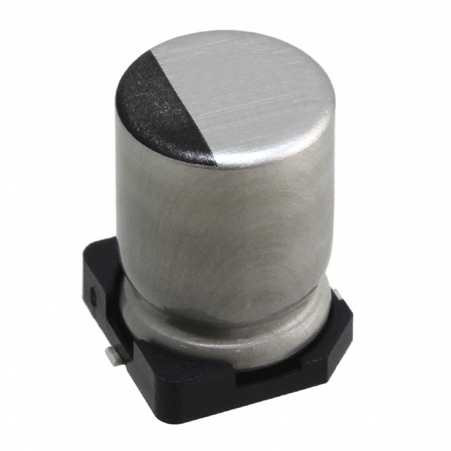
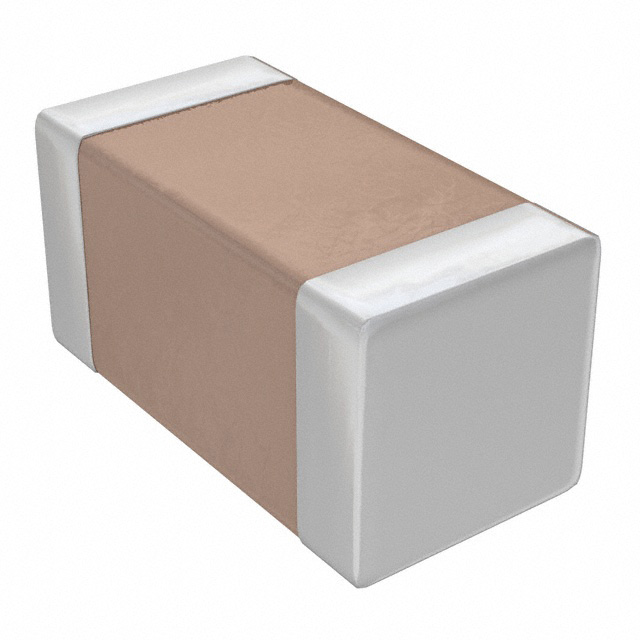
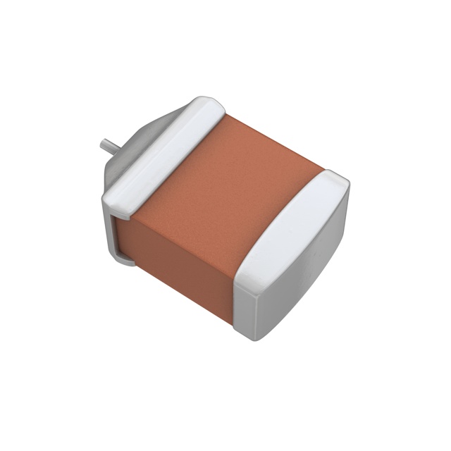
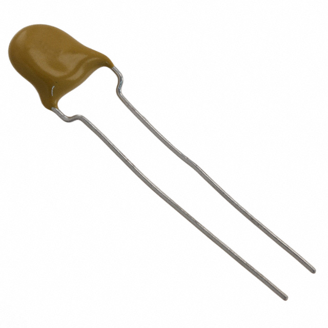
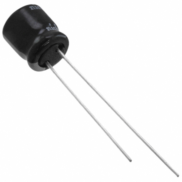
What Does a Memory Chip Look Like?
Memory chips come in many physical forms, ranging from simple and compact standalone chips to highly integrated modules. Their appearance can vary greatly depending on package type, external details, and size.
| Package Type | Appearance Description | Size Reference | Typical Applications |
|---|---|---|---|
| SOP / TSOP | A classic rectangular flat package with one or two rows of slender pins extending from both sides, similar to centipede legs. | A 44-TSOP SRAM chip may be about 10.16 mm wide and 18.41 mm long. | Early memory chips, NOR flash, SRAM, and related devices. |
| QFN / LGA / WSON | A pinless square or rectangular flat package with bottom pads or side contacts. | An SD NAND chip in an LGA-8 package may measure about 6 × 8 mm. | Embedded devices and compact flash memory chips. |
| BGA | A package with many tiny solder balls arranged on the bottom. No pins are visible from the outside. | A hybrid BGA memory chip may have a mainstream size such as 11.5 × 13 mm. | DRAM chips, high-end flash memory, eMMC, UFS, and similar devices. |
| WLCSP | An extremely compact package whose size is almost the same as the die itself. | It can be smaller than 1 × 1 mm, with a thickness of only about 0.25 mm. | Mobile devices and space-constrained electronics. |
| DIP | A classic black package with two parallel rows of metal pins on both sides. | Relatively large and commonly seen in older ROM chips. | Development boards, teaching experiments, and early computers. |
In finished products, memory chips may appear as RAM modules, SSDs, eMMC chips, UFS chips, BIOS flash chips, or compact embedded memory devices. Their shape depends on packaging, application, and integration level.
What Is a Flash Memory Chip?
A flash memory chip is a non-volatile storage device. Its core feature is that stored data is not lost when power is turned off. It can also be repeatedly erased and rewritten using electrical signals without replacing the chip.
The basic storage unit of flash memory is a special transistor structure. It stores digital data by controlling whether electrons enter or leave a storage region such as a floating gate or charge-trap layer.
NAND Flash vs. NOR Flash
- NAND flash memory: High density, fast writing, and relatively low cost. It is used in USB flash drives, SD cards, smartphone storage, and SSDs.
- NOR flash memory: Fast random reading and capable of direct code execution. It is used for BIOS, bootloaders, firmware, and embedded startup code.
Main Advantages
- Shock-resistant because it has no moving parts.
- Silent during operation.
- Small in size and lightweight.
- Low power consumption.
- Fast read and write speed, especially in SSD applications.
Main Limitations
- Flash memory has a limited erase/write lifespan.
- Long-term power-off data retention may degrade over time.
- The cost per unit capacity is usually higher than that of traditional mechanical hard drives.
Flash memory chips are a core storage technology in modern digital devices. They ensure that the apps on your phone and the operating system on your computer do not disappear after shutdown.
What Is a Memory Chip in a Computer?
A memory chip in a computer is a miniature electronic component made from semiconductor materials. It is used to store data and instructions. It acts like the computer’s “memory cells,” helping determine how much information a device can store and how quickly it can read and write data.
RAM Chips
RAM is extremely fast, but once power is cut off, all data stored in it disappears. It acts as a high-speed workbench for the CPU. Common RAM chips are usually DRAM devices soldered onto memory modules.
Flash Memory Chips
Flash memory is relatively fast and does not lose data when power is turned off. NAND flash is the core component of SSDs, USB drives, memory cards, and smartphone storage.
ROM and CMOS Memory
ROM stores basic firmware such as BIOS or UEFI startup programs. CMOS memory stores a very small amount of data, including system time and basic hardware configuration information.
| Feature | Memory Chip: RAM | Flash Memory Chip: NAND Flash |
|---|---|---|
| Volatile? | Yes. Data is lost when power is removed. | No. Data is retained after power is removed. |
| Speed | Extremely fast, often at the nanosecond level. | Fast, often at the microsecond level, but typically much slower than RAM. |
| Function | Runs programs and temporarily processes data. | Stores files, applications, and the operating system for the long term. |
| Where You See It | Computer memory modules and graphics card video memory. | SSDs, USB flash drives, memory cards, and smartphone storage chips. |
What Is On-Chip Memory?
On-chip memory is a storage unit integrated directly inside a chip. It is manufactured on the same silicon die as the core logic circuits of a CPU, GPU, microcontroller, or system-on-chip.
Core Features of On-Chip Memory
- Extremely high speed: It is very close to the CPU core and does not require long external bus transmission.
- Very low power consumption: Data movement inside the chip consumes less energy than off-chip access.
- Limited capacity: Chip area is expensive, so on-chip memory is usually small.
- Flexible structure: It can be designed as cache, dedicated RAM, tightly coupled memory, or scratchpad memory.
Common Types
- CPU cache: L1, L2, and L3 cache reduce the speed gap between the processor and main memory.
- MCU internal flash and SRAM: Used in microcontrollers such as STM32 and ESP32.
- TCM: Tightly coupled memory for deterministic real-time access.
- Scratchpad memory: Software-managed high-speed memory used in GPUs, DSPs, and specialized processors.
| Feature | On-Chip Memory | Off-Chip Memory |
|---|---|---|
| Location | Inside the CPU, GPU, MCU, or system-on-chip. | On the motherboard or in an external storage device. |
| Speed | Extremely fast. | Slower than on-chip memory. |
| Capacity | Small, usually from KB to MB. | Large, ranging from GB to TB depending on the memory or storage type. |
| Power Consumption | Lower for each data access. | Higher because signals travel through external buses and interfaces. |
| Typical Examples | CPU cache, MCU flash, MCU SRAM, TCM, scratchpad memory. | DDR DRAM modules, SSDs, NAND flash storage, hard drives. |
Overall, on-chip memory is the closest, fastest, and most limited storage layer in a computer system. It sacrifices capacity and cost efficiency in exchange for maximum speed, low latency, and energy efficiency.
Need Memory ICs for Your Project?
For electronic manufacturers, distributors, and engineering teams, choosing the right memory chip depends on capacity, speed, interface, package, endurance, operating temperature, and long-term supply availability.
View Memory Chip FAQFAQ About Memory Chips
1. What is a memory chip?
A memory chip is a semiconductor device used to store digital data. It may store temporary working data, permanent files, firmware, boot code, or hardware configuration settings.
2. What are memory chips mainly made of?
Most memory chips are mainly built on high-purity monocrystalline silicon wafers. They also contain metal interconnects, dielectric layers, dopants, photoresist-defined patterns, and packaging materials.
3. Are memory chips made directly from sand?
Not directly. Silicon can be derived from silica-rich materials such as sand, but chip manufacturing requires extensive purification, crystal growth, wafer slicing, polishing, and many nanoscale fabrication steps.
4. What is the difference between RAM and flash memory?
RAM is volatile and loses data when power is turned off. Flash memory is non-volatile and keeps data without power. RAM is used for running programs, while flash memory is used for long-term storage.
5. What data is stored in CMOS memory?
CMOS memory stores BIOS or UEFI settings, system time and date, boot order, hardware configuration parameters, power management options, and sometimes security settings.
6. What does a memory chip look like?
A memory chip usually looks like a small black rectangular or square component. Depending on the package, it may have visible pins, hidden solder balls, or flat metal pads.
7. Is an SSD a memory chip?
An SSD is not a single memory chip. It is a complete storage device containing multiple NAND flash chips, a controller chip, firmware, and sometimes cache memory.
8. Why do computers need different types of memory chips?
Different memory chips provide different advantages. Cache and SRAM are extremely fast but small. DRAM is suitable for working memory. NAND flash is large and non-volatile. ROM and CMOS store firmware and configuration data.
9. What is on-chip memory used for?
On-chip memory is used for extremely fast access to important data and instructions inside a processor. Examples include CPU cache, MCU SRAM, on-chip flash, TCM, and scratchpad memory.
10. Does flash memory wear out?
Yes. Flash memory has a limited number of erase and write cycles. Modern SSDs use wear leveling, error correction, and controller algorithms to extend service life.


.png?x-oss-process=image/format,webp/resize,h_32)


