
 German
 Japanese
 Portuguese
 Korea
Korea
 Mexico
 Dutch
Dutch


Transimpedance Amplifier: Turning Tiny Sensor Currents into Useful Signals (Without Losing Your Mind)

If you work with light sensors, photodiodes, PMTs, gas detectors, or any other component that spits out current instead of voltage, you’ve probably met a transimpedance amplifier already — maybe without realizing it. It’s the quiet character in the background of every “detect a single photon” movie scene, the unsung sidekick in lab instruments, and the reason your optical sensor board does anything at all.
In this guide we’re going to treat the transimpedance amplifier the way sci-fi treats a good support character: give it an origin story, show its hidden powers, and explain how it stays stable under ridiculous conditions.
We’ll cover:
- What a transimpedance amplifier actually is
- Why photodiodes and other sensors love it so much
- How to design the feedback network (Rf and Cf) like a pro
- Noise, bandwidth, and that never-ending tradeoff between “fast” and “low-noise”
- How to pick op-amps and passive components
- Layout, guarding, shielding, and all the real-world messy details
- Debugging common issues so your transimpedance amplifier doesn’t oscillate like a lightsaber
Sprinkled in: references to popular shows and movies, because debugging a transimpedance amplifier sometimes feels like trying to stabilize a starship core with duct tape and a multimeter.
1. What Is a Transimpedance Amplifier, Really?
Let’s start with the name.
Trans-impedance = “transfer impedance”.
A transimpedance amplifier is an amplifier whose job is to convert an input current into an output voltage. The standard equation you’ll see in nearly every datasheet is:
VOUT = −IIN × RF
You feed a small sensor current IIN into the inverting input of an op-amp, place a feedback resistor RF from output to input, and the transimpedance amplifier spits out a voltage proportional to that current. The minus sign just means it inverts — the world doesn’t end.
The classic architecture is:
- Sensor (often a photodiode) wired to the inverting input
- Non-inverting input tied to some reference (often ground or virtual ground)
- Feedback resistor RF (and sometimes a capacitor CF) from output back to inverting input
- Op-amp keeps its inputs at almost the same voltage, so the sensor “sees” a nearly constant bias while its current flows through RF
That’s it. A transimpedance amplifier is a current-to-voltage converter with gain in units of ohms (V/A = Ω). Simple on paper; surprisingly subtle in practice.
2. Where Transimpedance Amplifiers Show Up in Real Life
If this were Stranger Things, the transimpedance amplifier is the scientist in the lab who quietly explains the physics while everybody else screams about monsters.
You’ll find a transimpedance amplifier in:
- Photodiode receivers
- Ambient light sensors
- Optical smoke detectors
- Heart-rate monitoring (PPG green LED + photodiode)
- Fiber-optic communication receivers
- LIDAR and time-of-flight sensors
- Photomultiplier tubes (PMTs) and avalanche photodiodes (APDs)
- Medical imaging, nuclear instrumentation, fluorescence detection
- Gas and chemical sensors that output tiny currents proportional to concentration
- Charge-integrating detectors
- X-ray / gamma detectors
- Radiation dosimetry
- Precision current measurement
- Shunt-based current sensors for picoamp or nanoamp measurement
- “Guarded” current measurement setups in electrometers
Basically, whenever a sensor produces current and we want a clean voltage that an ADC, FPGA, or microcontroller can digest, a transimpedance amplifier is waiting in the wings.
.png?x-oss-process=image/auto-orient,1/quality,q_70/format,webp)
3. Anatomy of a Transimpedance Amplifier: The Minimal Circuit
Strip away all the marketing graphics and a transimpedance amplifier is really just an op-amp plus a feedback element.
3.1 The core circuit
- Op-amp
Ideally low input bias current, low noise, and enough gain-bandwidth to handle your sensor and RF. - Feedback resistor RF
Sets the transimpedance gain: VOUT / IIN = −RF.
Example: a 1 MΩ RF converts 1 µA into −1 V. - Feedback capacitor CF
Usually placed in parallel with RF. This tiny capacitor stabilizes the transimpedance amplifier by compensating for the input capacitance of the sensor plus op-amp. Without CF, your transimpedance amplifier can oscillate like a badly tuned guitar pedal. - Sensor (e.g., photodiode)
Connected in reverse bias (for speed) or photovoltaic mode (for low dark noise), feeding its current into the inverting node. - Reference for the non-inverting input
Often ground, but in many transimpedance amplifier designs you’ll use a “virtual ground” or mid-supply reference so you can swing the output above and below that point on a single-supply system.
3.2 Why not just use a resistor to ground?
You could take your current-output sensor, stick a resistor to ground, and measure the voltage across it with an ADC. But:
- The sensor voltage will vary as current changes, which can change its linearity and speed (especially for photodiodes).
- The sensor sees whatever noise your ADC input and supply lines throw at it.
- The transimpedance amplifier keeps the sensor node at a nearly constant voltage, which is like giving your sensor a quiet reading room instead of a noisy cafeteria.
That’s why essentially every serious optical front end uses a transimpedance amplifier rather than a simple resistor.
4. Transimpedance Amplifier + Photodiode: The Classic Duo
Photodiodes and transimpedance amplifiers are the MCU and GPIO of the analog sensing world: they show up together everywhere.
4.1 Photodiode modes
A photodiode can be used in:
- Photovoltaic mode (zero bias or small forward voltage)
- Lowest noise
- Narrow bandwidth
- Good for slow, very low light measurements (light meters, precision detectors)
- Photoconductive mode (reverse bias)
- Increased depletion region, lower capacitance
- Faster response, higher bandwidth
- Higher dark current noise
In both modes, the photodiode current is roughly proportional to the incident light. The transimpedance amplifier:
- Keeps the photodiode voltage nearly constant
- Turns that current into a voltage at its output
- Decides the tradeoff between gain (RF) and bandwidth
4.2 Bandwidth vs gain
A painful but fundamental truth of transimpedance amplifier design:
Higher RF → higher gain, but lower bandwidth.
Bandwidth roughly scales with the op-amp’s gain-bandwidth product (GBW) divided by RF and the total input capacitance (sensor + op-amp + layout). If you want:
- High gain AND
- High bandwidth
…you need a very fast op-amp (high GBW), small sensor capacitance, a carefully chosen CF, and very clean PCB layout.
Designing high-speed transimpedance amplifiers for gigabit fiber is like building the Millennium Falcon: fast, temperamental, and heavily dependent on the wiring.

5. Noise in a Transimpedance Amplifier: Where the Hiss Comes From
If your application is about seeing a few photons in a dark lab or tracking tiny currents, noise is the main villain.
A transimpedance amplifier’s noise budget includes:
- Photodiode shot noise
Proportional to the square root of the DC photocurrent (plus dark current).
Fundamental, can’t be “designed away”; you can only minimize it by reducing dark current and unnecessary bias. - Feedback resistor noise (Johnson / thermal noise)
RF generates voltage noise density of √(4 kT RF).
Higher RF = higher gain but also higher noise.
Thin-film, low-noise resistors are preferred in precision transimpedance amplifiers. - Op-amp voltage noise
Appears at the input and gets multiplied by noise gain (not just RF!).
For large RF, voltage noise often dominates at high frequencies. - Op-amp current noise
Flows through RF and creates additional noise.
Especially critical when RF is very large (megaohms–gigaohms) and when dealing with picoamp currents. - Capacitive noise peaking
Input capacitances plus CF and RF shape the noise spectrum; poorly compensated transimpedance amplifiers can show noise peaking near the bandwidth limit.
If this sounds like the villains’ roster from a Marvel movie, that’s because designing a quiet transimpedance amplifier really is about managing multiple antagonists at once.
5.1 Practical noise-reduction tips
- Keep RF only as large as necessary for your required output swing and ADC range.
- Use low-noise, low-leakage resistors and avoid carbon composition parts.
- Choose op-amps with:
- Low voltage noise for low RF
- Low current noise for high RF
- Minimize capacitance at the inverting node with compact layout and short sensor leads.
- Shield the front end from EMI, use proper grounding, and avoid digital traces near the transimpedance amplifier input.
6. Choosing the Right Op-Amp and Components for a Transimpedance Amplifier
Designing a transimpedance amplifier is 30% math, 30% reading datasheets, 40% layout, and 10% coffee. Yes, that’s 110%; analog design always feels like it’s over budget.
6.1 Op-amp selection checklist
When you pick an op-amp for a transimpedance amplifier, consider:
- Gain-bandwidth product (GBW)
Must be comfortably higher than your target transimpedance bandwidth.
For high-speed photodiode interfaces, you’re often in the hundreds of MHz or multi-GHz GBW territory. - Input bias current
Directly corrupts your measurement when dealing with picoamps–nanoamps.
FET-input or CMOS op-amps are typical for ultra-low current transimpedance amplifier designs. - Input voltage and current noise
There’s always a tradeoff; high-speed bipolar op-amps may have higher current noise but extremely low voltage noise. - Input capacitance
Adds to the photodiode capacitance and affects stability & bandwidth.
Specified as common-mode and differential input capacitances. - Supply voltage and output swing
Ensure the transimpedance amplifier can swing enough output voltage without clipping, especially with single-supply systems. - Package and thermal considerations
For high-speed or high-power transimpedance amplifier ICs, pay attention to package thermal pad, soldering, and layout recommendations.
6.2 Feedback resistor and capacitor
The feedback network defines your transimpedance amplifier’s personality.
- RF value
Set by required gain: VOUT,max / IIN,max.
Add headroom so you don’t hit rail at peak current. - RF technology
Use thin-film or metal-film with low noise and good tempco.
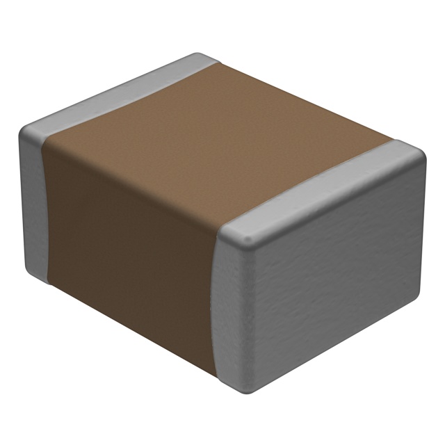
Avoid large through-hole leads that add unnecessary parasitic capacitance. - CF value
Typically chosen to ensure phase margin and flat frequency response.
Initial estimate often uses CF ≈ CIN / (2π × GBW × RF²) (rough guideline, refine with simulation).
6.3 Passive components around the transimpedance amplifier
Support components matter:
- Input protection (small series resistor, clamping diodes) for harsh environments
- RC output filters to limit broadband noise going into the ADC
- Biasing networks for photodiodes to set correct reverse voltage
In well-designed boards, you can identify the transimpedance amplifier section as the tiny, meticulously routed island with guard rings and an unusually high component-to-copper ratio.

7. Stability of a Transimpedance Amplifier: Fighting Oscillation
A transimpedance amplifier is inherently less stable than a simple inverting amplifier because of the extra capacitance at its input. The photodiode capacitance, op-amp input capacitance, and stray layout capacitance all create a pole that can eat into your phase margin.
7.1 The main stability enemies
- Photodiode capacitance (CD) – can be 1–100 pF or more
- Op-amp input capacitances (CIN+, CIN−)
- Feedback capacitance (CF, intentional)
- Stray capacitance from long traces, solder pads, test points
Put them together and your transimpedance amplifier looks like a multi-pole system, which can easily oscillate if the op-amp GBW is high and CF is too small.
7.2 Compensation strategy
- Start from op-amp application notes for transimpedance amplifier stability. Most big vendors show formulas linking RF, CF, and total input capacitance.
- Use SPICE simulation with an accurate model of the op-amp, photodiode capacitance, and feedback network.
- Aim for at least 45–60° phase margin. Flatter than a Marvel multiverse timeline is not required, but you don’t want ringing.
- Add a small resistor in series with the photodiode in high-speed systems if necessary to tame parasitics (at the cost of a bit of noise/bandwidth).
7.3 Symptom: your transimpedance amplifier oscillates
- Output shows a high-frequency sine wave or ringing even in the dark
- Noise floor looks like a mountain range on your spectrum analyzer
- The scope trace of a step input overshoots and rings
Fixes often include increasing CF, shortening high-impedance traces, lowering RF, or even choosing an op-amp with slightly lower GBW.
8. PCB Layout for a Transimpedance Amplifier: Where Heroes Are Made
You can have the perfect transimpedance amplifier schematic and still get a “why is this oscillating at 40 MHz” horror story because of layout.
8.1 Keep the inverting node tiny
- The inverting input of the transimpedance amplifier is a high-impedance, sensitive node.
- Keep the copper around it microscopic.
- Run the feedback components (RF, CF) directly to it with the shortest possible loop.
8.2 Guard rings and leakage control
When you’re dealing with picoamps or femtoamps:
- Use guard rings connected to a low-impedance potential at the same voltage as the input node.
- Keep solder mask openings minimal; flux residue can leak.
- Consider using Teflon standoffs, high-resistance materials, and clean boards.
8.3 Grounding strategy
- Provide a solid ground reference near the transimpedance amplifier but keep digital grounds and high current paths away from the sensitive input region.
- Sometimes using an analog ground island with a single connection to system ground reduces noise.
8.4 Decoupling and supply routing
- Place decoupling capacitors as close as physically possible to op-amp supply pins.
- Use multiple caps (e.g., 100 nF + 1 µF) to cover a wide frequency range.
- Route supply lines away from the inverting input and feedback traces to minimize coupling.
If you look at high-end transimpedance amplifier evaluation boards from IC vendors, you’ll notice they often look like tiny RF boards: short traces, controlled loops, and carefully separated analog/digital areas.

9. Practical Design Examples of Transimpedance Amplifiers
Let’s walk through three representative transimpedance amplifier scenarios.
9.1 Low-speed, high-gain photodiode transimpedance amplifier
Use case: ambient light sensor for a smart home device
- Photodiode current range: 10 pA to 1 µA
- Desired output: 0–2 V into an ADC
- Target bandwidth: a few kHz (it’s just room lighting)
Design choices:
- Use a CMOS op-amp with picoamp input bias current and GBW of a few MHz.
- Set RF ≈ 2 MΩ (1 µA → 2 V).
- Add a modest CF to set bandwidth ~1–5 kHz and ensure stability with the photodiode’s capacitance.
- PCB layout emphasizes leakage control and shielding from 50/60 Hz mains noise.
This transimpedance amplifier is the analog equivalent of a calm character in a drama series: not fast, not flashy, but extremely reliable.
9.2 High-speed fiber-optic transimpedance amplifier
Use case: multi-hundred-Mbps optical receiver
- Photodiode current pulses with fast rise times
- Bandwidth: tens to hundreds of MHz
- Gain: enough to feed a limiting amplifier or comparator
Design choices:
- Select a high-GBW op-amp (hundreds of MHz or GHz) or use a dedicated TIA IC designed for optical comms.
- RF is small (kΩ range) to maintain high bandwidth.
- CF is carefully optimized, sometimes dominated by parasitics.
- Differential outputs may be used for better noise immunity.
Layout is treated like high-frequency RF: controlled impedance traces, symmetrical routing, and minimal stub lengths. This transimpedance amplifier is more The Flash than The Godfather.
9.3 MCU-friendly transimpedance amplifier for a low-cost sensor
Use case: gas sensor board feeding an STM32 ADC
- Sensor outputs tiny currents proportional to gas concentration
- Bandwidth: a few tens of Hz (gas diffusion is slow)
- System powered from 3.3 V, restricted BOM
Design choices:
- General-purpose low-noise op-amp with GBW around 5–10 MHz.
- RF chosen to map max gas current to ~2.5 V output.
- Optional output RC filter (e.g., 1 kΩ + 100 nF) before ADC to avoid aliasing.
- Single-supply transimpedance amplifier with virtual ground at ~1.65 V.
This is the “embedded everyman” transimpedance amplifier: not glamorous, but present in millions of sensor nodes across IoT and industrial systems.
10. Integrated Transimpedance Amplifier ICs vs Discrete Designs
You can build a transimpedance amplifier from a vanilla op-amp + RF + CF + photodiode, or you can use an integrated transimpedance amplifier IC that wraps many of these inside.
10.1 Pros of integrated transimpedance amplifier ICs
- Optimized for stability with specified sensor capacitance ranges
- Built-in gain stages, AGC (automatic gain control), or limiting amplifiers
- Often include noise-optimized feedback networks and on-chip resistors
- Smaller board area, fewer external components, well-documented application circuits
These are popular in optical communications, medical instrumentation, and high-volume sensors where performance and size matter.
10.2 Pros of discrete transimpedance amplifier designs
- Full control over RF, CF, and op-amp type
- Easier to tweak for unusual sensors or custom bandwidth/noise tradeoffs
- Cheaper in low/medium performance situations
- Educational value — you actually learn how a transimpedance amplifier behaves
For many real-world projects, teams start with a discrete transimpedance amplifier during R&D, then later migrate to an integrated transimpedance amplifier IC or custom ASIC once requirements solidify.

11. Debugging a Misbehaving Transimpedance Amplifier
Let’s say your transimpedance amplifier is acting like a chaotic character from Rick and Morty instead of a calm analog circuit. What now?
11.1 Symptom: output stuck at rail
Likely causes:
- Dark current or background light is larger than expected → RF too high
- Input offset or bias current of the op-amp is creating a large DC output
- Photodiode wired in the wrong polarity
Fixes:
- Reduce RF, or add offset compensation
- Check dark current and shield the sensor
- Verify photodiode anode/cathode orientation
11.2 Symptom: excessive noise
Likely causes:
- Too-large RF causing high Johnson noise
- Noisy op-amp choice for given gain
- Poor shielding, digital noise coupling into the inverting node
- Oscillation near the bandwidth limit
Fixes:
- Use a lower-noise op-amp or lower RF and add gain in a later stage
- Improve ground, shielding, and decoupling
- Check with a scope for oscillation; adjust CF
11.3 Symptom: ringing or oscillation
Likely causes:
- Under-compensated transimpedance amplifier (CF too small)
- Excess input capacitance from long sensor cables
- Op-amp GBW too high for the chosen RF and CIN
Fixes:
- Increase CF slightly and re-measure step response
- Shorten leads, reduce capacitance, or use coax with proper termination
- Use op-amp application note guidelines for transimpedance amplifier stability
11.4 Symptom: strange offsets over temperature
Likely causes:
- Feedback resistor has high temperature coefficient
- Op-amp input bias current drifts strongly with temperature
- Leakage paths changing with humidity or contamination
Fixes:
- Use precision, low-tempco RF
- Choose a better op-amp or implement background calibration
- Clean the board thoroughly and possibly conformally coat it
12. Wrapping Up: Why the Transimpedance Amplifier Deserves More Love
The transimpedance amplifier is one of those circuits that looks trivial in a textbook and then consumes an entire week of your life when you try to make it work on a real PCB with real sensors and real noise.
Key takeaways:
- A transimpedance amplifier converts sensor current to a usable voltage while keeping the sensor at a stable bias.
- It’s essential for photodiodes, PMTs, gas sensors, and any ultra-low current measurement.
- Op-amp selection, RF, CF, and sensor capacitance together set gain, bandwidth, noise, and stability.
- Good PCB layout and guarding are as important as the schematic.
- Debugging a misbehaving transimpedance amplifier usually boils down to: “too much gain,” “not enough compensation,” or “too much capacitance where you didn’t expect it.”
Once you’ve tamed your first transimpedance amplifier, you’ll start seeing it everywhere — from medical instruments and fiber links to that tiny heart-rate sensor on your smartwatch. It may not be flashy, but like the best supporting characters in big franchises, a well-designed transimpedance amplifier quietly carries the plot.
13. Transimpedance Amplifier FAQ
Q1: When should I use a transimpedance amplifier instead of a simple shunt resistor?
Use a transimpedance amplifier whenever your sensor is primarily a current source and you care about either linearity, bandwidth, or very small currents. A plain resistor to ground lets the sensor voltage swing with current, which can change its characteristics and invite noise. A transimpedance amplifier keeps the sensor node at a nearly constant voltage while cleanly converting current to voltage.
Q2: How do I choose the feedback resistor value RF?
Start from your maximum expected sensor current and your desired maximum output voltage. RF ≈ VOUT,max / IIN,max. Then check whether the resulting bandwidth, noise, and op-amp input specifications are acceptable. If not, adjust RF, choose a different op-amp, or add another gain stage downstream.
Q3: Why does my transimpedance amplifier oscillate when I connect the photodiode with a long cable?
The cable adds capacitance at the inverting input, which reduces phase margin and can push the transimpedance amplifier into oscillation. Use shorter leads, use a coax cable with proper termination, or increase the feedback capacitor CF to restore stability. In very high-speed systems, a small series resistor at the photodiode or cable end can also help tame parasitics.
Q4: Is it better to put gain in the transimpedance amplifier or in a following voltage amplifier stage?
It’s usually best to give the transimpedance amplifier only as much gain as you need for a clean signal and then add extra gain in a second, lower-impedance stage. Very large RF values increase noise, reduce bandwidth, and make stability harder. Splitting gain between the transimpedance amplifier and a later stage can yield a cleaner, more stable system.
Q5: Can I build a transimpedance amplifier on a breadboard?
You can prototype extremely low-speed, low-gain transimpedance amplifiers on a breadboard, but high-speed or low-current designs will suffer from excessive stray capacitance and leakage. For anything serious, move the transimpedance amplifier to a proper PCB with short traces, a solid ground, and good guarding and decoupling practices.

 FAQ
FAQ


.png?x-oss-process=image/format,webp/resize,h_32)


