
 German
 Japanese
 Portuguese
 Korea
Korea
 Mexico
 Dutch
Dutch


Why Choose Us?
Professional Platform
B2B & B2C purchasingDelivery at full speed
1-2 days deliveryWide variety
Original manufacturers365 days guarantee
Responsible quality
.png)


Tech Specifications
XC7A35T-L1CSG324I Description
XC7A35T-L1CSG324I Overview
The XC7A35T-L1CSG324I FPGA boasts a capacity of 35,000 logic cells, rendering it an ideal choice for smaller-scale designs and applications. The "L1" designation in the model name denotes its speed grade, indicating that it operates at a moderate performance level.
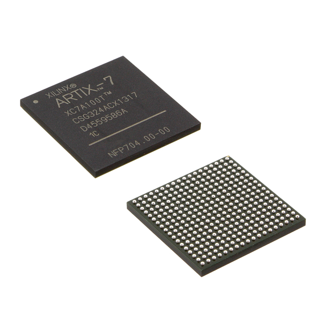
This FPGA is available in a chip-scale grid array (CSGA) package type known as CSG324I, which features 324 pins. This package type offers a compact form factor that facilitates seamless integration into various systems and applications.
Thanks to its moderate logic cell count and performance level, the XC7A35T-L1CSG324I FPGA is well-suited for applications that require a balance between complexity and resource utilization. It is particularly useful in areas such as digital signal processing, embedded systems, and low-power applications, where efficient and dependable performance is critical.
XC7A35T-L1CSG324I Features
Partial Reconfiguration
Low-Power Optimization
High-Level Synthesis (HLS)
Heterogeneous System Integration
XC7A35T-L1CSG324I Applications
Software-defined radio
Video & Image Processing
Aircraft navigation
Wireless Technology
FAQ
| Quantity | Unit Price | Ext. Price |
|---|---|---|
| 1+ | $62.21600 | $62.22 |
Not available to buy online? Want the lower wholesale price? Please Send RFQ to get best price, we will respond immediately


.png?x-oss-process=image/format,webp/resize,h_32)


