

Not available to buy online? Want the lower wholesale price? Please Send RFQ to get best price, we will respond immediately


.png?x-oss-process=image/format,webp/resize,p_30)


XC7A100T-1FTG256I Description
XC7A100T-1FTG256I Overview
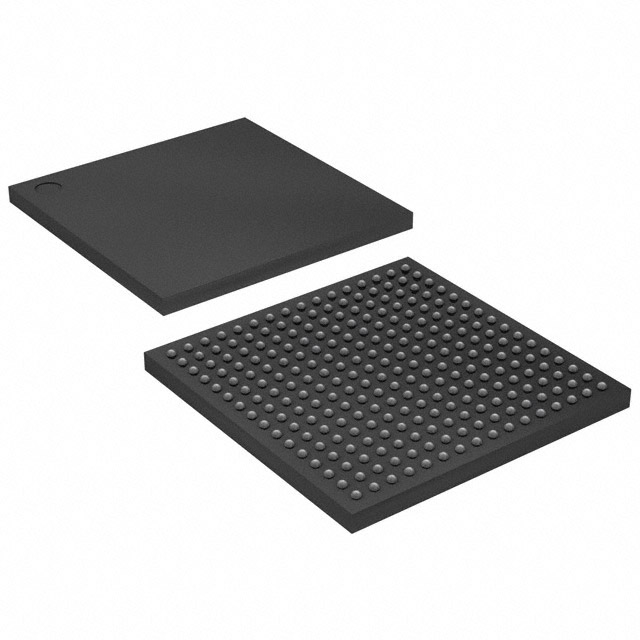
For improved data transfer, there are 358 I/Os. There are 43661 logic elements/cells in the basic building blocks of logic. A power supply voltage of 1.2V volts is required for the device to function. This FPGA module can be connected to the development board using Surface Mount connections. The battery in this device is 1.14V1.26V. When operating the machine, it is critical to keep the operating temperature within the range of 0°C85°C TJ. This device is equipped with 358 outputs. This FPGA model has been packed in Tray to conserve space.
XC7A100T-1FTG256I Features
Low-cost, wire-bond, bare-die flip-chip, and high signal integrity flip chip packaging offering easy migration between family members in the same package. All packages available in Pb-free and selected packages in Pb option.
Designed for high performance and lowest power with 28 nm, HKMG, HPL process, 1.0V core voltage process technology and 0.9V core voltage option for even lower power.
36 Kb dual-port block RAM with built-in FIFO logic for on-chip data buffering.
High-performance SelectIO™ technology with support for DDR3 interfaces up to 1,866 Mb/s.
XC7A100T-1FTG256I Applications
Wireless Technology
Industrial Control
Internet of Things
Medical Equipment
Consumer Electronics
Tech Specifications
XC7A100T-1FTG256I Documents
Download datasheets and manufacturer documentation for XC7A100T-1FTG256I
 XC7A100T/200T Errata 7 Series FPGA Overview Artix-7 FPGAs Datasheet Artix-7 FPGAs Brief Xilinx REACH211 Cert Xiliinx RoHS Cert
 Related Parts


Relevant Search
Shopping Guide


.png?x-oss-process=image/format,webp/resize,h_32)


©2025 ERSA Electronics Corporation.