

Not available to buy online? Want the lower wholesale price? Please Send RFQ to get best price, we will respond immediately


- 1+
- $20.84904
- $20.85
- 10+
- $20.00448
- $200.04
- 30+
- $18.54223
- $556.27

.png?x-oss-process=image/format,webp/resize,p_30)


XC7A50T-2FGG484C Description
XC7A50T-2FGG484C Overview
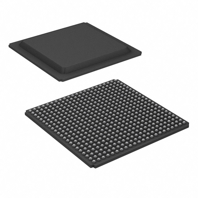
Xilinx FPGAXC7A50T-2 FGGG484C is a programmable chip with superior performance, making it ideal for a wide range of applications. The device has 250 I/O ports for more consistent data transmission. The base component consists of 52160 logic elements/cells. To operate FPGA chips, 1V volts voltage supply is required. The FPGA part is the Field Programmable Gate Arrays family as part of the programmable gate array family. An accessory Surface Mount allows the FPGA module to be attached to the development board. FPGA chips operate stopgap chips with a supply voltage of 0.95V to 1.05V. As part of the Artix-7 series of Gasps, it is a type of FPGA. Gaff chips is necessary to keep the operating temperature stopgap chip shin 0°C~85°C TJ when the device is operating. During the installation of the device, 250 outputs were incorporated. Unlike other FPGA models, this one is contained in Tray to space saving.
XC7A50T-2FGG484C Features
High-speed serial connectivity with built-in multi-gigabit transceivers from 600 Mb/s to max rates of 6.6 Gb/s up to 28.05 Gb/s, offering a special low-power mode, optimized for chip-to-chip interfaces.
A user configurable analog interface (XADC), incorporating dual 12-bit 1MSPS analog-to-digital converters with on-chip thermal and supply sensors.
Powerful clock management tiles (CMT), combining phase-locked loop (PLL) and mixed-mode clock manager (MMCM) blocks for high precision and low jitter.
Quickly deploy embedded processing with MicroBlaze™ processor.
XC7A50T-2FGG484C Applications
Medical Equipment
Consumer Electronics
Aerospace & Defense
Telecommunication
Wireless Communications
Tech Specifications
XC7A50T-2FGG484C Documents
Download datasheets and manufacturer documentation for XC7A50T-2FGG484C
 7 Series FPGAs PCB Design Guide Artix-7 FPGAs Datasheet Artix-7 FPGAs Brief Xilinx REACH211 Cert Xiliinx RoHS Cert
 Related Parts


Relevant Search
Shopping Guide


.png?x-oss-process=image/format,webp/resize,h_32)


©2025 ERSA Electronics Corporation.