
 German
 Japanese
 Portuguese
 Korea
Korea
 Mexico
 Dutch
Dutch


Why Choose Us?
Professional Platform
B2B & B2C purchasingDelivery at full speed
1-2 days deliveryWide variety
Original manufacturers365 days guarantee
Responsible quality
.png)


Tech Specifications
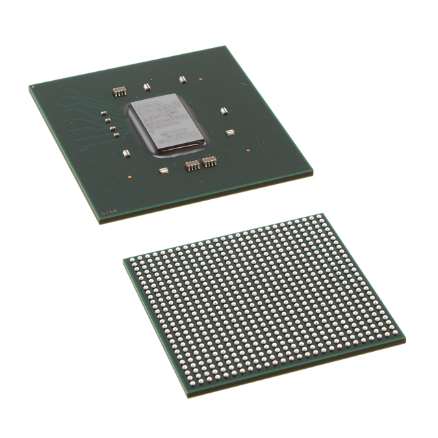
XC7Z030-1FBG676I Description
The XC7Z030-1FBG676I is a Field Programmable Gate Array (FPGA) device manufactured by AMD (previously known as Xilinx). It belongs to the Zynq-7000 series, which combines the capabilities of a general-purpose processor with the flexibility of an FPGA. Here's a description, features, and potential applications for the XC7Z030-1FBG676I:
Description:
The XC7Z030-1FBG676I is a mid-range FPGA device that offers a balance between performance, power consumption, and cost. It is designed to be used in a wide range of applications where a combination of processing power and reconfigurable logic is required.
Features:
- Integration: The device integrates a central processing unit (CPU) with reconfigurable logic, allowing for both general-purpose processing and custom hardware acceleration.
- Processing Power: It features a single-core processor based on the ARM Cortex-A9 architecture, capable of handling various processing tasks.
- Logic Cells: The FPGA fabric consists of configurable logic blocks (CLBs) that can be programmed to implement custom digital logic functions.
- Memory: The device includes block RAM (BRAM) for data storage and various memory controllers to interface with external memory.
- I/O: It offers a variety of I/O options, including high-speed transceivers, GPIOs, and interfaces for connecting to other peripherals.
- Connectivity: The XC7Z030-1FBG676I supports various communication protocols, such as Ethernet, USB, and PCI Express, for seamless integration with other systems.
- Power Efficiency: The device is designed to operate with low power consumption, making it suitable for battery-powered or energy-sensitive applications.
- Reconfigurability: As an FPGA, the XC7Z030-1FBG676I can be reprogrammed in the field, allowing for updates and modifications to its functionality throughout its lifecycle.
Applications:
- Industrial Automation: The XC7Z030-1FBG676I can be used in control systems for robotic arms, assembly lines, or other automated machinery.
- Video Processing: Its combination of processing power and reconfigurable logic makes it suitable for video processing applications, such as image recognition, encoding, or decoding.
- Medical Devices: The device can be used in medical imaging equipment, patient monitoring systems, or other medical devices that require real-time processing and control.
- Communications: It can be employed in networking equipment, such as routers, switches, or base stations, where high-speed data processing and forwarding are required.
- Automotive: The XC7Z030-1FBG676I can be used in advanced driver-assistance systems (ADAS), infotainment systems, or other automotive applications that demand a combination of processing and custom logic.
- Aerospace and Defense: The device can be utilized in aerospace and defense applications, such as signal processing, radar systems, or secure communications, where reliability and reconfigurability are crucial.
- Test and Measurement: The FPGA's flexibility makes it suitable for test and measurement equipment, where custom logic can be implemented to handle specific testing requirements.
In summary, the XC7Z030-1FBG676I is a versatile FPGA device that combines processing power with reconfigurable logic, making it suitable for a wide range of applications where both capabilities are required. Its features, such as low power consumption, connectivity options, and reconfigurability, make it an attractive choice for various industries and applications.
FAQ
| Quantity | Unit Price | Ext. Price |
|---|---|---|
| 1+ | $329.47200 | $329.47 |
Not available to buy online? Want the lower wholesale price? Please Send RFQ to get best price, we will respond immediately


.png?x-oss-process=image/format,webp/resize,h_32)


