
 German
 Japanese
 Portuguese
 Korea
Korea
 Mexico
 Dutch
Dutch


Infineon Technologies
CY2CC1810OI

Why Choose Us?
Professional Platform
B2B & B2C purchasingDelivery at full speed
1-2 days deliveryWide variety
Original manufacturers365 days guarantee
Responsible quality
.png)


Tech Specifications
CY2CC1810OI Description
CY2CC1810OI Description
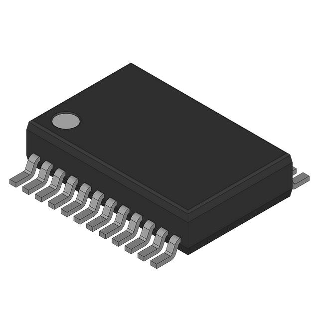
The CY2CC1810OI is a high-performance clock buffer IC designed for distributing clock signals with minimal skew and jitter. Manufactured by Cypress Semiconductor Corp and distributed by Infineon Technologies, this device is categorized under Clock/Timing ICs. It features a 1:10 fanout ratio, making it ideal for applications requiring multiple clock outputs from a single input source. The CY2CC1810OI operates within a supply voltage range of 2.375V to 2.625V and 3.135V to 3.465V, ensuring compatibility with various power supply configurations. It supports LVCMOS and LVTTL input levels and provides AVCMOS output levels, making it versatile for different circuit designs. The device is housed in a surface-mount 24SSOP package, which is ideal for compact and high-density PCB layouts.
CY2CC1810OI Features
- High Fanout Ratio: The 1:10 fanout ratio allows the CY2CC1810OI to distribute a single clock signal to up to ten output lines, reducing the need for multiple buffer stages and simplifying circuit design.
- Wide Operating Voltage Range: With a supply voltage range of 2.375V to 2.625V and 3.135V to 3.465V, the CY2CC1810OI can operate efficiently in various power supply environments, enhancing its flexibility in different applications.
- Low Skew and Jitter: The CY2CC1810OI is designed to minimize skew and jitter, ensuring precise and reliable clock signal distribution. This is crucial for maintaining signal integrity in high-frequency applications.
- Surface-Mount Packaging: The 24SSOP package is suitable for surface-mount technology (SMT), allowing for high-density PCB layouts and efficient manufacturing processes.
- High Maximum Frequency: With a maximum operating frequency of 200 MHz, the CY2CC1810OI is well-suited for high-speed clock distribution in modern electronic systems.
- Moisture Sensitivity Level (MSL) 1: The CY2CC1810OI has an MSL rating of 1, indicating it is not moisture-sensitive and can be stored and handled without special precautions, reducing the risk of damage during manufacturing processes.
CY2CC1810OI Applications
The CY2CC1810OI is ideal for a variety of applications where reliable and efficient clock signal distribution is required. Some specific use cases include:
- Telecommunications: In base stations and network equipment, the CY2CC1810OI can distribute clock signals to multiple components, ensuring synchronized operation and minimizing signal degradation.
- Data Centers: For server and storage systems, the device can provide stable clock signals to multiple processors and memory modules, enhancing system performance and reliability.
- Consumer Electronics: In devices such as routers, switches, and set-top boxes, the CY2CC1810OI can distribute clock signals to various subsystems, ensuring accurate timing and reducing electromagnetic interference.
- Industrial Automation: In control systems and PLCs, the device can distribute clock signals to multiple sensors and actuators, ensuring precise timing and synchronization.
Conclusion of CY2CC1810OI
The CY2CC1810OI is a robust and versatile clock buffer IC that offers significant advantages over similar models. Its high fanout ratio, wide operating voltage range, and low skew and jitter performance make it an ideal choice for a wide range of applications. The surface-mount 24SSOP package and MSL 1 rating further enhance its suitability for modern manufacturing processes. Whether used in telecommunications, data centers, consumer electronics, or industrial automation, the CY2CC1810OI provides reliable and efficient clock signal distribution, ensuring optimal system performance and reliability.
FAQ
Not available to buy online? Want the lower wholesale price? Please Send RFQ to get best price, we will respond immediately


.png?x-oss-process=image/format,webp/resize,h_32)


