
 German
 Japanese
 Portuguese
 Korea
Korea
 Mexico
 Dutch
Dutch


Infineon Technologies
CY2PD817ZC

Why Choose Us?
Professional Platform
B2B & B2C purchasingDelivery at full speed
1-2 days deliveryWide variety
Original manufacturers365 days guarantee
Responsible quality
.png)


Tech Specifications
CY2PD817ZC Description
CY2PD817ZC Description
The CY2PD817ZC is a high-performance clock buffer designed by Cypress Semiconductor Corp, now part of Infineon Technologies. This device is specifically engineered to provide reliable and efficient clock distribution in various electronic systems. Operating within a temperature range of 0°C to 85°C (TA), the CY2PD817ZC is suitable for a wide range of industrial and commercial applications.
The CY2PD817ZC features a 1:7 fanout ratio, allowing it to distribute a single input clock signal to seven output signals. This makes it ideal for applications where multiple clock signals are required to drive various components within a system. The device supports differential signaling for both input and output, ensuring high signal integrity and reduced electromagnetic interference (EMI). The input is designed to accept LVPECL (Low Voltage Positive Emitter Coupled Logic) signals, while the outputs can be configured to provide LVCMOS, LVPECL, or LVTTL (Low Voltage Transistor-Transistor Logic) signals, offering flexibility in interfacing with different types of digital circuits.
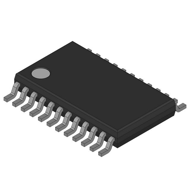
With a maximum operating frequency of 320 MHz, the CY2PD817ZC is capable of handling high-speed clock signals, making it suitable for modern, high-performance systems. The device operates from a supply voltage range of 2.375V to 2.625V, ensuring compatibility with various power supply configurations. The CY2PD817ZC is available in a surface-mount 24-TSSOP package, which is ideal for compact and dense PCB layouts.
CY2PD817ZC Features
- Operating Temperature Range: 0°C to 85°C (TA), ensuring reliable performance across a broad temperature spectrum.
- ECCN Classification: EAR99, indicating compliance with export regulations.
- Fanout Ratio: 1:7, providing efficient clock distribution to multiple destinations.
- Differential Signaling: Supports differential input and output, enhancing signal integrity and reducing EMI.
- Input and Output Compatibility: Accepts LVPECL input and provides LVCMOS, LVPECL, or LVTTL outputs, offering versatile interfacing options.
- High-Speed Operation: Capable of handling clock signals up to 320 MHz, suitable for high-performance applications.
- Supply Voltage Range: 2.375V to 2.625V, ensuring compatibility with a variety of power supply configurations.
- Surface-Mount Packaging: 24-TSSOP package, ideal for compact and dense PCB layouts.
- Moisture Sensitivity Level: MSL 1 (Unlimited), indicating robustness against moisture-related issues during manufacturing and storage.
CY2PD817ZC Applications
The CY2PD817ZC is well-suited for a variety of applications where reliable and efficient clock distribution is critical. Some specific use cases include:
- High-Speed Communication Systems: Distributing clock signals to multiple components in high-speed data communication systems, ensuring synchronized operation.
- Telecommunications: Providing clock signals to various modules in telecommunication equipment, maintaining signal integrity and reducing EMI.
- Data Centers: Distributing clock signals to multiple servers and storage devices, ensuring synchronized operation and data integrity.
- Industrial Automation: Providing reliable clock signals to various control systems and sensors, ensuring accurate timing and control.
- Consumer Electronics: Distributing clock signals to various components in consumer electronics, such as televisions, gaming consoles, and multimedia devices.
Conclusion of CY2PD817ZC
The CY2PD817ZC is a robust and versatile clock buffer that offers high performance and reliability in clock distribution. Its unique features, such as differential signaling, wide operating frequency range, and flexible output configurations, make it a superior choice over similar models. The device's compatibility with various power supply configurations and its surface-mount packaging further enhance its suitability for modern electronic systems. Whether used in high-speed communication systems, telecommunication equipment, data centers, industrial automation, or consumer electronics, the CY2PD817ZC ensures efficient and reliable clock distribution, making it an essential component for any system requiring precise timing and synchronization.
FAQ
| Quantity | Unit Price | Ext. Price |
|---|---|---|
| 33+ | $7.95520 | $262.52 |
Not available to buy online? Want the lower wholesale price? Please Send RFQ to get best price, we will respond immediately


.png?x-oss-process=image/format,webp/resize,h_32)


