

Intel
5CGXFC7D6F31C6N
FPGAs

Not available to buy online? Want the lower wholesale price? Please Send RFQ to get best price, we will respond immediately


.png?x-oss-process=image/format,webp/resize,p_30)


5CGXFC7D6F31C6N Description
5CGXFC7D6F31C6N Description
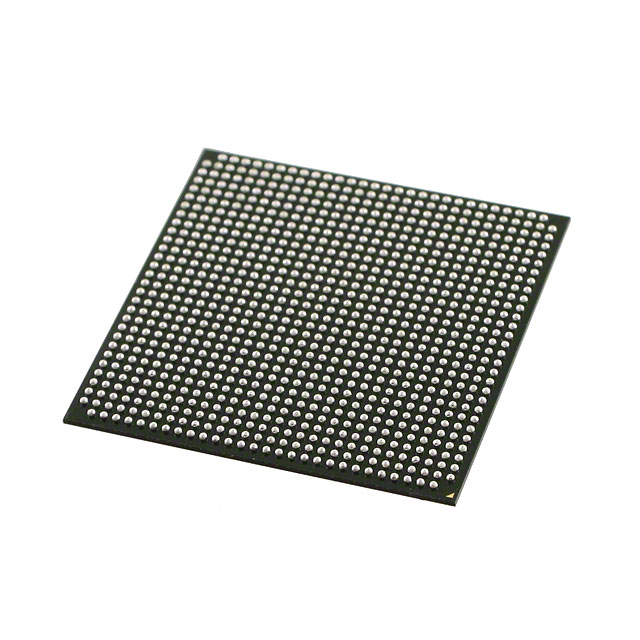
The 5CGXFC7D6F31C6N is a high-performance Field Programmable Gate Array (FPGA) from Intel's Cyclone® V GX series, designed to deliver exceptional computational power and flexibility. This FPGA is ideal for a wide range of applications requiring high I/O counts and robust processing capabilities. With 480 I/Os and a total of 7,880,704 RAM bits, the 5CGXFC7D6F31C6N offers substantial memory and connectivity options. It features 56,480 Logic Array Blocks (LABs) or Configurable Logic Blocks (CLBs), and 149,500 logic elements or cells, providing extensive programmable logic resources. The device operates within a supply voltage range of 1.07V to 1.13V and can function reliably in an operating temperature range of 0°C to 85°C (TJ). The 5CGXFC7D6F31C6N is available in an 896-pin Fine Ball Grid Array (FBGA) package, making it suitable for surface mount applications. It is RoHS compliant and REACH unaffected, ensuring environmental and regulatory compliance. The device is shipped in a tray package and has a moisture sensitivity level (MSL) of 3 (168 hours).
5CGXFC7D6F31C6N Features
- High I/O Count: With 480 I/Os, the 5CGXFC7D6F31C6N is well-suited for applications requiring extensive connectivity and interfacing with multiple peripherals.
- Substantial Memory: The device offers a total of 7,880,704 RAM bits, providing ample memory for complex operations and data storage.
- Extensive Programmable Logic: The 56,480 LABs/CLBs and 149,500 logic elements/cells provide significant programmable logic resources, enabling the implementation of complex algorithms and designs.
- Reliable Operation: The operating temperature range of 0°C to 85°C (TJ) ensures stable performance in various environmental conditions.
- Efficient Power Management: The supply voltage range of 1.07V to 1.13V helps in maintaining low power consumption while ensuring high performance.
- Compliance and Reliability: The RoHS compliance and REACH unaffected status ensure that the device meets environmental and regulatory standards. The MSL of 3 (168 hours) indicates its reliability in moisture-sensitive environments.
- Surface Mount Compatibility: The 896FBGA package is ideal for surface mount applications, making it suitable for modern, space-constrained designs.
5CGXFC7D6F31C6N Applications
The 5CGXFC7D6F31C6N is versatile and can be deployed in a variety of applications, including:
- Telecommunications: Ideal for base stations, switches, and other communication infrastructure requiring high I/O and processing capabilities.
- Industrial Automation: Suitable for programmable logic controllers (PLCs), motor controls, and other industrial applications where robust processing and connectivity are essential.
- Automotive: Can be used in advanced driver-assistance systems (ADAS), infotainment systems, and other automotive electronics requiring high performance and reliability.
- Medical Devices: Applicable in medical imaging, diagnostic equipment, and other medical applications where precision and reliability are critical.
- Consumer Electronics: Suitable for high-end consumer devices requiring significant processing power and connectivity, such as smart TVs and gaming consoles.
Conclusion of 5CGXFC7D6F31C6N
The 5CGXFC7D6F31C6N FPGA from Intel's Cyclone® V GX series is a powerful and versatile device, offering a combination of high I/O count, substantial memory, and extensive programmable logic resources. Its reliable operation within a wide temperature range and efficient power management make it suitable for a variety of demanding applications. The device's compliance with environmental and regulatory standards ensures its suitability for modern, environmentally conscious designs. With its surface mount compatibility and robust performance, the 5CGXFC7D6F31C6N is an excellent choice for engineers and designers looking for a reliable and high-performance FPGA solution.
Tech Specifications
5CGXFC7D6F31C6N Documents
Download datasheets and manufacturer documentation for 5CGXFC7D6F31C6N
Cyclone V GX,GT,E Errata Cyclone V Device Datasheet Cyclone V Device Overview Mult Dev Label Chgs 24/Feb/2020 Mult Dev Label CHG 24/Jan/2020 Virtual JTAG Megafuntion Guide Cyclone V Device Handbook Datasheet Update 09/Aug/2023 Mult PN LABEL 01/08/2023 Related Parts


Shopping Guide


.png?x-oss-process=image/format,webp/resize,h_32)


©2025 ERSA Electronics Corporation.