
 German
 Japanese
 Portuguese
 Korea
Korea
 Mexico
 Dutch
Dutch


Intel
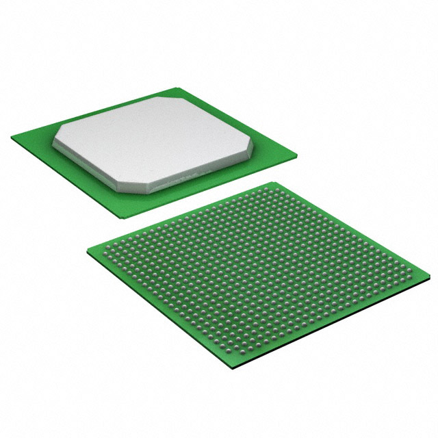
EP2C35F672C8

Why Choose Us?
Professional Platform
B2B & B2C purchasingDelivery at full speed
1-2 days deliveryWide variety
Original manufacturers365 days guarantee
Responsible quality
.png)


Tech Specifications
EP2C35F672C8 Description
The Intel EP2C35F672C8 is a field programmable gate array (FPGA) device that belongs to the Cyclone II family. This device is designed to provide high performance, low power consumption, and a wide range of features for various applications.
Description:
The EP2C35F672C8 is a mid-range FPGA that offers a balance between performance, power consumption, and cost. It is based on Intel's low-power 65nm process technology and features a high-density architecture that allows for efficient implementation of complex digital systems.
Features:
- Performance: The EP2C35F672C8 offers a maximum performance of 301 MHz, which is suitable for a wide range of applications that require moderate processing power.
- Logic Elements: The device contains 35,280 logic elements (LEs) that can be used to implement various digital logic functions.
- Memory Resources: The EP2C35F672C8 includes 34 Megabytes (Mb) of on-chip block RAM, which can be used for data storage and processing.
- I/O Resources: The device provides 672 I/O pins, which can be configured for various functions such as input/output, JTAG, and clock signals.
- DSP Blocks: The FPGA includes 180 digital signal processing (DSP) blocks, which can be used for high-speed data processing and arithmetic operations.
- Low Power Consumption: The EP2C35F672C8 is designed for low power operation, making it suitable for battery-powered and energy-efficient applications.
- Security Features: The device offers security features such as secure device configuration and bitstream encryption to protect intellectual property and ensure data integrity.
Applications:
The Intel EP2C35F672C8 is suitable for a wide range of applications due to its balance of performance, power consumption, and features. Some potential applications include:
- Communications: The device can be used in communication systems such as base stations, routers, and switches, where high-speed data processing and low latency are required.
- Industrial Automation: The EP2C35F672C8 can be used in industrial control systems, where real-time processing, data acquisition, and actuator control are necessary.
- Video Processing: The FPGA can be employed in video processing applications, such as image and video compression, decompression, and streaming.
- Medical Imaging: The device can be used in medical imaging systems for image processing, analysis, and display.
- Automotive: The EP2C35F672C8 can be utilized in automotive applications, such as advanced driver assistance systems (ADAS) and infotainment systems, where real-time processing and low power consumption are crucial.
- Aerospace and Defense: The FPGA can be employed in aerospace and defense applications, such as signal processing, radar systems, and secure communication systems.
In summary, the Intel EP2C35F672C8 is a versatile FPGA device that offers a balance of performance, power consumption, and features, making it suitable for a wide range of applications in various industries.
FAQ
Not available to buy online? Want the lower wholesale price? Please Send RFQ to get best price, we will respond immediately


.png?x-oss-process=image/format,webp/resize,h_32)


