
 German
 Japanese
 Portuguese
 Korea
Korea
 Mexico
 Dutch
Dutch


Intel
EP3C80F484I7N

Why Choose Us?
Professional Platform
B2B & B2C purchasingDelivery at full speed
1-2 days deliveryWide variety
Original manufacturers365 days guarantee
Responsible quality
.png)


Tech Specifications
EP3C80F484I7N Description
Intel's EP3C80F484I7N is a high-performance field-programmable gate array (FPGA) that belongs to the Cyclone III family. This device is designed to provide a combination of high-density integration, low power consumption, and high performance, making it suitable for a wide range of applications.
Description:
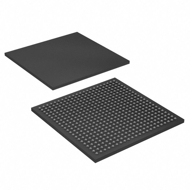
The EP3C80F484I7N is a mid-range FPGA that features a high-density of programmable logic elements, making it ideal for complex digital designs. It has a total of 80,000 logic elements and 484 I/O pins, providing a high level of integration and flexibility for system designers. The device is available in a flip-chip ball grid array (FCBGA) package, which allows for high-density mounting and improved thermal performance.
Features:
- High-density programmable logic elements: The EP3C80F484I7N features 80,000 logic elements, providing a high level of integration for complex digital designs.
- 484 I/O pins: The device has a large number of I/O pins, allowing for a wide range of interface options and flexibility in system design.
- Low power consumption: The Cyclone III family is designed for low power operation, making it suitable for battery-powered or energy-sensitive applications.
- High-performance transceivers: The device includes high-performance transceivers that can support data rates up to 3.5 Gbps, making it suitable for high-speed communication applications.
- Embedded memory: The EP3C80F484I7N includes a variety of embedded memory options, including block RAM and distributed RAM, providing flexible memory solutions for digital designs.
- Digital signal processing (DSP) capabilities: The device includes dedicated DSP blocks that can be used for high-speed mathematical operations, making it suitable for applications that require intensive signal processing.
Applications:
The EP3C80F484I7N is suitable for a wide range of applications that require high-density integration, low power consumption, and high performance. Some potential applications include:
- Communications infrastructure: The high-speed transceivers and DSP capabilities make the EP3C80F484I7N suitable for use in communication systems, such as routers, switches, and base stations.
- Industrial control systems: The device's flexibility and I/O options make it well-suited for industrial control applications, such as motor control, sensor interfacing, and data acquisition.
- Automotive systems: The EP3C80F484I7N can be used in automotive applications, such as infotainment systems, advanced driver assistance systems (ADAS), and powertrain control.
- Consumer electronics: The device's low power consumption and high performance make it suitable for use in consumer electronics, such as set-top boxes, gaming consoles, and smart home devices.
- Aerospace and defense: The EP3C80F484I7N can be used in aerospace and defense applications, such as radar systems, satellite communications, and electronic warfare systems.
In summary, the Intel EP3C80F484I7N is a high-performance, mid-range FPGA that offers a combination of high-density integration, low power consumption, and high performance. Its features and capabilities make it suitable for a wide range of applications, including communications infrastructure, industrial control systems, automotive systems, consumer electronics, and aerospace and defense.
FAQ
Not available to buy online? Want the lower wholesale price? Please Send RFQ to get best price, we will respond immediately


.png?x-oss-process=image/format,webp/resize,h_32)


